SBAS444E May   2009  – December 2024 ADS1113 , ADS1114 , ADS1115

PRODUCTION DATA  

  1.   1
  2. Features
  3. Applications
  4. Description
  5.   Device Comparison Table
  6. Pin Configuration and Functions
  7. Specifications
    1. 5.1 Absolute Maximum Ratings
    2. 5.2 ESD Ratings
    3. 5.3 Recommended Operating Conditions
    4. 5.4 Thermal Information
    5. 5.5 Electrical Characteristics
    6. 5.6 Timing Requirements: I2C
    7. 5.7 Typical Characteristics
  8. Parameter Measurement Information
    1. 6.1 Noise Performance
  9. Detailed Description
    1. 7.1 Overview
    2. 7.2 Functional Block Diagrams
    3. 7.3 Feature Description
      1. 7.3.1 Multiplexer
      2. 7.3.2 Analog Inputs
      3. 7.3.3 Full-Scale Range (FSR) and LSB Size
      4. 7.3.4 Voltage Reference
      5. 7.3.5 Oscillator
      6. 7.3.6 Output Data Rate and Conversion Time
      7. 7.3.7 Digital Comparator (ADS1114 and ADS1115 Only)
      8. 7.3.8 Conversion Ready Pin (ADS1114 and ADS1115 Only)
      9. 7.3.9 SMbus Alert Response
    4. 7.4 Device Functional Modes
      1. 7.4.1 Reset and Power-Up
      2. 7.4.2 Operating Modes
        1. 7.4.2.1 Single-Shot Mode
        2. 7.4.2.2 Continuous-Conversion Mode
      3. 7.4.3 Duty Cycling For Low Power
    5. 7.5 Programming
      1. 7.5.1 I2C Interface
        1. 7.5.1.1 I2C Address Selection
        2. 7.5.1.2 I2C General Call
        3. 7.5.1.3 I2C Speed Modes
      2. 7.5.2 Target Mode Operations
        1. 7.5.2.1 Receive Mode
        2. 7.5.2.2 Transmit Mode
      3. 7.5.3 Writing To and Reading From the Registers
      4. 7.5.4 Data Format
  10. Registers
    1. 8.1 Register Map
      1. 8.1.1 Address Pointer Register (address = N/A) [reset = N/A]
      2. 8.1.2 Conversion Register (P[1:0] = 00b) [reset = 0000h]
      3. 8.1.3 Config Register (P[1:0] = 01b) [reset = 8583h]
      4. 8.1.4 Lo_thresh (P[1:0] = 10b) [reset = 8000h] and Hi_thresh (P[1:0] = 11b) [reset = 7FFFh] Registers
  11. Application and Implementation
    1. 9.1 Application Information
      1. 9.1.1 Basic Connections
      2. 9.1.2 Single-Ended Inputs
      3. 9.1.3 Input Protection
      4. 9.1.4 Unused Inputs and Outputs
      5. 9.1.5 Analog Input Filtering
      6. 9.1.6 Connecting Multiple Devices
      7. 9.1.7 Quick-Start Guide
    2. 9.2 Typical Application
      1. 9.2.1 Design Requirements
      2. 9.2.2 Detailed Design Procedure
        1. 9.2.2.1 Shunt Resistor Considerations
        2. 9.2.2.2 Operational Amplifier Considerations
        3. 9.2.2.3 ADC Input Common-Mode Considerations
        4. 9.2.2.4 Resistor (R1, R2, R3, R4) Considerations
        5. 9.2.2.5 Noise and Input Impedance Considerations
        6. 9.2.2.6 First-Order RC Filter Considerations
        7. 9.2.2.7 Circuit Implementation
        8. 9.2.2.8 Results Summary
      3. 9.2.3 Application Curves
  12. 10Power Supply Recommendations
    1. 10.1 Power-Supply Sequencing
    2. 10.2 Power-Supply Decoupling
  13. 11Layout
    1. 11.1 Layout Guidelines
    2. 11.2 Layout Example
  14. 12Device and Documentation Support
    1. 12.1 Documentation Support
      1. 12.1.1 Related Documentation
    2. 12.2 Receiving Notification of Documentation Updates
    3. 12.3 Support Resources
    4. 12.4 Trademarks
    5. 12.5 Electrostatic Discharge Caution
    6. 12.6 Glossary
  15. 13Revision History
  16. 14Mechanical, Packaging, and Orderable Information

Typical Characteristics

at TA = 25°C, VDD = 3.3V, FSR = ±2.048V, DR = 8SPS (unless otherwise noted)
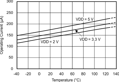
ADS1113 ADS1114 ADS1115 Operating Current vs Temperature
 
Figure 5-2 Operating Current vs Temperature
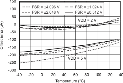
ADS1113 ADS1114 ADS1115 Single-Ended Offset Error vs Temperature
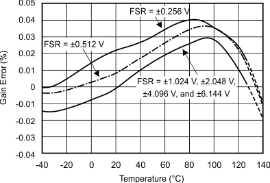
 
Figure 5-4 Single-Ended Offset Error vs Temperature
ADS1113 ADS1114 ADS1115 Gain Error vs Temperature
 
Figure 5-6 Gain Error vs Temperature
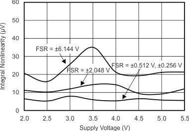
ADS1113 ADS1114 ADS1115 INL vs Supply Voltage
 
Figure 5-8 INL vs Supply Voltage
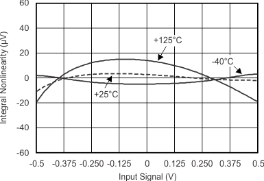
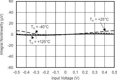
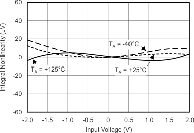
ADS1113 ADS1114 ADS1115 INL vs Input Signal
VDD = 3.3V, FSR = ±0.512V, DR = 8SPS, best fit
Figure 5-10 INL vs Input Signal
ADS1113 ADS1114 ADS1115 INL vs Input Signal
VDD = 5V, FSR = ±0.512V, DR = 8SPS, best fit
Figure 5-12 INL vs Input Signal
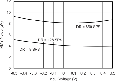
ADS1113 ADS1114 ADS1115 Noise vs Input Signal
FSR = ±0.512V
Figure 5-14 Noise vs Input Signal
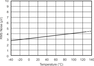
ADS1113 ADS1114 ADS1115 Noise vs Temperature
FSR = ±2.048V, DR = 8SPS
 
Figure 5-16 Noise vs Temperature
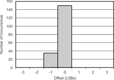
ADS1113 ADS1114 ADS1115 Offset Histogram
FSR = ±2.048V, 185 units
Figure 5-18 Offset Histogram
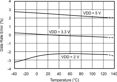
ADS1113 ADS1114 ADS1115 Data Rate vs Temperature
 
Figure 5-20 Data Rate vs Temperature
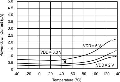
ADS1113 ADS1114 ADS1115 Power-Down Current vs Temperature
 
Figure 5-3 Power-Down Current vs Temperature
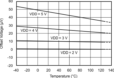
ADS1113 ADS1114 ADS1115 Differential Offset Error vs Temperature
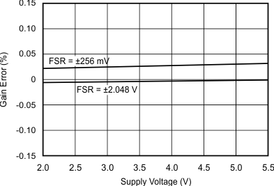
 
Figure 5-5 Differential Offset Error vs Temperature
ADS1113 ADS1114 ADS1115 Gain Error vs Supply Voltage
 
Figure 5-7 Gain Error vs Supply Voltage
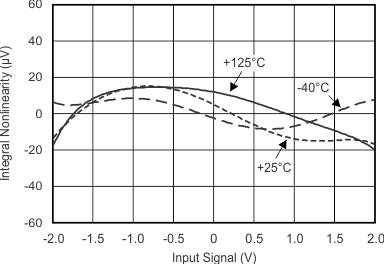
ADS1113 ADS1114 ADS1115 INL vs Input Signal
VDD = 3.3V, FSR = ±2.048V, DR = 8SPS, best fit
Figure 5-9 INL vs Input Signal
ADS1113 ADS1114 ADS1115 INL vs Input Signal
VDD = 5V, FSR = ±2.048V, DR = 8SPS, best fit
Figure 5-11 INL vs Input Signal
ADS1113 ADS1114 ADS1115 INL vs Temperature
 
Figure 5-13 INL vs Temperature
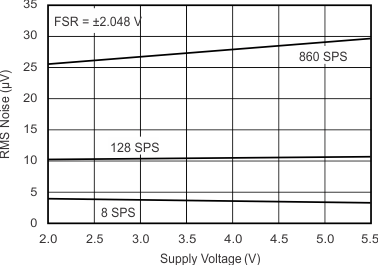
ADS1113 ADS1114 ADS1115 Noise vs Supply Voltage
FSR = ±2.048V
Figure 5-15 Noise vs Supply Voltage
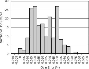
ADS1113 ADS1114 ADS1115 Gain Error Histogram
FSR = ±2.048V, 185 units
Figure 5-17 Gain Error Histogram
ADS1113 ADS1114 ADS1115 Total
                        Error vs Input Signal
Differential inputs; includes noise, offset and gain error
Figure 5-19 Total Error vs Input Signal
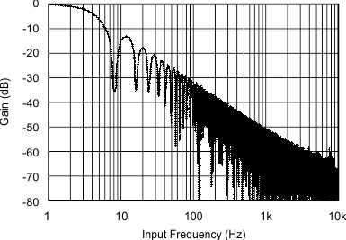
ADS1113 ADS1114 ADS1115 Digital Filter Frequency Response
DR = 8SPS
Figure 5-21 Digital Filter Frequency Response