SBAS486F November 2009 – February 2016 ADS41B29 , ADS41B49
PRODUCTION DATA.
- 1 Features
- 2 Applications
- 3 Description
- 4 Revision History
- 5 Pin Configuration and Functions
-
6 Specifications
- 6.1 Absolute Maximum Ratings
- 6.2 ESD Ratings
- 6.3 Recommended Operating Conditions
- 6.4 Thermal Information
- 6.5 Electrical Characteristics: General
- 6.6 Electrical Characteristics: ADS41B29, ADS41B49
- 6.7 Digital Characteristics
- 6.8 Timing Requirements: LVDS and CMOS Modes
- 6.9 Timing Requirements: Reset
- 6.10 Timing Requirements: LVDS Timing Across Sampling Frequencies
- 6.11 Timing Requirements: CMOS Timing Across Sampling Frequencies
- 6.12 Timing Requirements: CMOS Timing Across Sampling Frequencies
- 6.13 Typical Characteristics: ADS41B49
- 6.14 Typical Characteristics: ADS41B29
- 6.15 Typical Characteristics: General
- 6.16 Typical Characteristics: Contour
- 7 Parameter Measurement Information
-
8 Detailed Description
- 8.1 Overview
- 8.2 Functional Block Diagram
- 8.3 Feature Description
- 8.4 Device Functional Modes
- 8.5 Programming
- 8.6
Register Maps
- 8.6.1
Serial Register Map
- 8.6.1.1 Summary of High-Performance Modes
- 8.6.1.2
Description of Serial Registers
- 8.6.1.2.1 Register Address 00h (address = 00h) [reset = 00h]
- 8.6.1.2.2 Register Address 01h (address = 01h) [reset = 00h]
- 8.6.1.2.3 Register Address 03h (address = 03h) [reset = 00h]
- 8.6.1.2.4 Register Address 25h (address = 25h) [reset = 50h]
- 8.6.1.2.5 Register Address 26h (address = 26h) [reset = 00h]
- 8.6.1.2.6 Register Address 3Dh (address = 3Dh) [reset = 00h]
- 8.6.1.2.7 Register Address 3Fh (address = 3Fh) [reset = 00h]
- 8.6.1.2.8 Register Address 40h (address = 40h) [reset = 00h]
- 8.6.1.2.9 Register Address 41h (address = 41h) [reset = 00h]
- 8.6.1.2.10 Register Address 42h (address = 42h) [reset = 08h]
- 8.6.1.2.11 Register Address 43h (address = 43h) [reset = 00h]
- 8.6.1.2.12 Register Address 4Ah (address = 4Ah) [reset = 00h]
- 8.6.1.2.13 Register Address BFh (address = BFh) [reset = 00h]
- 8.6.1.2.14 Register Address CFh (address = CFh) [reset = 00h]
- 8.6.1.2.15 Register Address DFh (address = DFh) [reset = 00h]
- 8.6.1
Serial Register Map
- 9 Application and Implementation
- 10Power Supply Recommendations
- 11Layout
- 12Device and Documentation Support
- 13Mechanical, Packaging, and Orderable Information
7 Parameter Measurement Information
7.1 Timing Diagrams

1. With external 100-Ω termination.
Figure 48. LVDS Output Voltage Levels

1. At higher sampling frequencies, tDPI is greater than one clock cycle which then makes the overall latency = ADC latency + 1.
2. E = Even bits (D0, D2, D4, and so forth). O = Odd bits (D1, D3, D5, and so forth).
Figure 49. Latency Diagram

1. Dn = bits D0, D2, D4, and so forth. Dn + 1 = Bits D1, D3, D5, and so forth.
Figure 50. LVDS Mode Timing

Dn = bits D0, D1, D2, and so forth.
Figure 51. CMOS Mode Timing

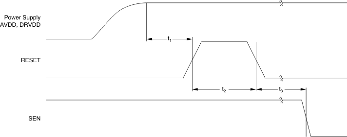
NOTE: A high pulse on the RESET pin is required in the serial interface mode in case of initialization through hardware reset. For parallel interface operation, RESET must be permanently tied high.
Figure 52. Reset Timing Diagram