SBAS520C February 2011 – June 2017 ADS4122 , ADS4125 , ADS4142 , ADS4145
PRODUCTION DATA.
- 1 Features
- 2 Applications
- 3 Description
- 4 Revision History
- 5 Device Family Comparison
- 6 Pin Configuration and Functions
-
7 Specifications
- 7.1 Absolute Maximum Ratings
- 7.2 ESD Ratings
- 7.3 Recommended Operating Conditions
- 7.4 Thermal Information
- 7.5 Electrical Characteristics: ADS412x
- 7.6 Electrical Characteristics: ADS414x
- 7.7 Electrical Characteristics: General
- 7.8 Digital Characteristics
- 7.9 Timing Requirements: LVDS and CMOS Modes
- 7.10 Serial Interface Timing Characteristics
- 7.11 Reset Timing Requirements
- 7.12 Timing Characteristics at Lower Sampling Frequencies
- 7.13 Typical Characteristics: ADS4122
- 7.14 Typical Characteristics: ADS4125
- 7.15 Typical Characteristics: ADS4142
- 7.16 Typical Characteristics: ADS4145
- 7.17 Typical Characteristics: Common
- 7.18 Typical Characteristics: Contour
- 8 Detailed Description
- 9 Application and Implementation
- 10Power Supply Recommendations
- 11Layout
- 12Device and Documentation Support
- 13Mechanical, Packaging, and Orderable Information
9 Application and Implementation
NOTE
Information in the following applications sections is not part of the TI component specification, and TI does not warrant its accuracy or completeness. TI’s customers are responsible for determining suitability of components for their purposes. Customers should validate and test their design implementation to confirm system functionality.
9.1 Application Information
The ADS412x and ADS414x are lower sampling speed members of the ADS41xx family of ultra-low-power analog-to-digital converters (ADCs). The conversion process is initiated by a rising edge of the external input clock and the analog input signal is sampled. The sampled signal is sequentially converted by a series of small resolution stages, with the outputs combined in a digital correction logic block. At every clock edge the sample propagates through the pipeline, resulting in a data latency of 10 clock cycles. The output is available as 14-bit data or 12-bit data, in DDR LVDS mode or CMOS mode, and coded in either straight offset binary or binary twos complement format.
9.1.1 Analog Input
The analog input consists of a switched-capacitor-based, differential, sample-and-hold architecture. This differential topology results in very good ac performance even for high input frequencies at high sampling rates. The INP and INM pins must be externally biased around a common-mode voltage of 0.95 V, available on the VCM pin. For a full-scale differential input, each input INP and INM pin must swing symmetrically between (VCM + 0.5 V) and (VCM – 0.5 V), resulting in a 2-VPP differential input swing. The input sampling circuit has a high
3-dB bandwidth that extends up to 550 MHz (measured from the input pins to the sampled voltage). Figure 105 shows an equivalent circuit for the analog input.
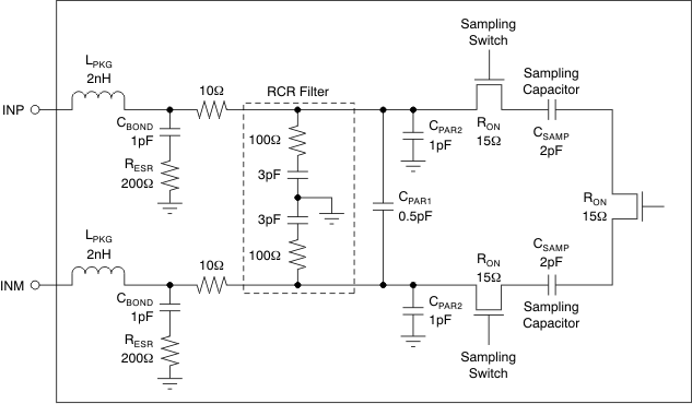 Figure 105. Analog Input Equivalent Circuit
9.1.1.1 Drive Circuit Requirements
For optimum performance, the analog inputs must be driven differentially. This technique improves the common-mode noise immunity and even-order harmonic rejection. A 5-Ω to 15-Ω resistor in series with each input pin is recommended to damp out ringing caused by package parasitics. Low impedance (less than 50 Ω) must be present for the common-mode switching currents. This impedance can be achieved by using two resistors from each input terminated to the common-mode voltage (VCM).
Note that the device includes an internal R-C filter from each input to ground. The purpose of this filter is to absorb the glitches caused by the opening and closing of the sampling capacitors. The cutoff frequency of the R-C filter involves a trade-off. A lower cutoff frequency (larger C) absorbs glitches better, but also reduces the input bandwidth and the maximum input frequency that can be supported. On the other hand, with no internal R-C filter, high input frequency can be supported but now the sampling glitches must be supplied by the external driving circuit. The inductance of the package bond wires limits the ability of the external driving circuit to support the sampling glitches.
In the ADS412x and ADS414x, the R-C component values are optimized when supporting high input bandwidth (550 MHz). However, in applications where very high input frequency support is not required, filtering of the glitches can be improved further with an external R-C-R filter; see Figure 108 and Figure 109).
In addition, the drive circuit may have to be designed to provide a low insertion loss over the desired frequency range and matched impedance to the source. When designing the drive circuit, the ADC impedance must be considered. Figure 106 and Figure 107 show the impedance (ZIN = RIN || CIN) looking into the ADC input pins.
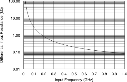 Figure 106. ADC Analog Input Resistance (RIN) Across Frequency
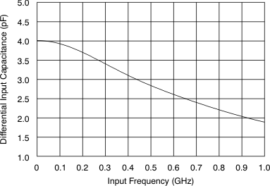 Figure 107. ADC Analog Input Capacitance (CIN) Across Frequency
9.1.1.2 Driving Circuit
Two example driving circuit configurations are shown in Figure 108 and Figure 109—one optimized for low bandwidth (low input frequencies) and the other one for high bandwidth to support higher input frequencies. In Figure 108, an external R-C-R filter with 3.3 pF is used to help absorb sampling glitches. The R-C-R filter limits the bandwidth of the drive circuit, making the drive circuit suitable for low input frequencies (up to 250 MHz). Transformers such as ADT1-1WT or WBC1-1 can be used up to 250 MHz.
For higher input frequencies, the R-C-R filter can be dropped. Together with the lower series resistors (5 Ω to 10 Ω), this drive circuit provides higher bandwidth to support frequencies up to 500 MHz (as shown in Figure 109). A transmission line transformer such as ADTL2-18 can be used.
Note that both the drive circuits have been terminated by 50 Ω near the ADC side. The termination is accomplished by a 25-Ω resistor from each input to the 0.95-V common-mode (VCM) from the device. This termination allows the analog inputs to be biased around the required common-mode voltage.
 Figure 108. Drive Circuit With Low Bandwidth (for Low Input Frequencies)
 Figure 109. Drive Circuit With High Bandwidth (for High Input Frequencies)
The mismatch in the transformer parasitic capacitance (between the windings) results in degraded even-order harmonic performance. Connecting two identical RF transformers back-to-back helps minimize this mismatch and good performance is obtained for high-frequency input signals. An additional termination resistor pair may be required between the two transformers, as shown in Figure 108 and Figure 109. The center point of this termination is connected to ground to improve the balance between the P (positive) and M (negative) sides. The values of the terminations between the transformers and on the secondary side must be chosen to obtain an effective 50 Ω (for a 50-Ω source impedance).
Figure 108 and Figure 109 use 1:1 transformers with a 50-Ω source. As explained in the Drive Circuit Requirements section, this architecture helps to present a low source impedance to absorb sampling glitches. With a 1:4 transformer, the source impedance is 200 Ω. The higher source impedance is unable to absorb the sampling glitches effectively and can lead to degradation in performance (compared to using 1:1 transformers).
In almost all cases, either a band-pass or low-pass filter is needed to obtain the desired dynamic performance, as shown in Figure 110. Such a filter presents low source impedance at the high frequencies corresponding to the sampling glitch and helps avoid the performance loss with the high source impedance.
 Figure 110. Drive Circuit With 1:4 Transformer
9.1.1.3 Input Common-Mode
To ensure a low-noise, common-mode reference, the VCM pin is filtered with a 0.1-µF low-inductance capacitor connected to ground. The VCM pin is designed to directly drive the ADC inputs. Each ADC input pin sinks a common-mode current of approximately 0.6 µA per MSPS of clock frequency.
9.1.2 Clock Input
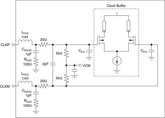
The ADS412x and ADS414x clock inputs can be driven differentially (sine, LVPECL, or LVDS) or single-ended (LVCMOS), with little or no difference in performance between them. The common-mode voltage of the clock inputs is set to VCM using internal 5-kΩ resistors. This setting allows the use of transformer-coupled drive circuits for sine-wave clock or ac-coupling for LVPECL and LVDS clock sources. Figure 111 shows an equivalent circuit for the input clock.
A single-ended CMOS clock can be ac-coupled to the CLKP input, with CLKM connected to ground with a 0.1-μF capacitor, as shown in Figure 112. For best performance, the clock inputs must be driven differentially, reducing susceptibility to common-mode noise. For high input frequency sampling, TI recommends using a clock source with very low jitter. Band-pass filtering of the clock source can help reduce the effects of jitter. There is no change in performance with a non-50% duty cycle clock input. Figure 113 shows a differential circuit.
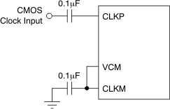 Figure 112. Single-Ended Clock Driving Circuit
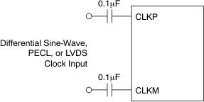 Figure 113. Differential Clock Driving Circuit
9.1.3 Input Overvoltage Indication (OVR Pin)
The device has an OVR pin that provides information about analog input overload. At any clock cycle, if the sampled input voltage exceeds the positive or negative full-scale range, the OVR pin goes high. The OVR remains high as long as the overload condition persists. The OVR pin is a CMOS output buffer (running off DRVDD supply), independent of the type of output data interface (DDR, LVDS, or CMOS).
For a positive overload, the D[13:0] output data bits are 3FFFh in offset binary output format and 1FFFh in twos complement output format. For a negative input overload, the output code is 0000h in offset binary output format and 2000h in twos complement output format.
9.1.4 Using the ADS41xx at Low Sampling Rates
When ADS41xx is used at lower sampling rates (< 20 MSPS), set the LOW SPEED register bit (address DFh, bit[5:4]). At low sampling rates, use the device in CMOS interface mode which saves power and results in better setup and hold time compared to LVDS interface mode.
9.1.4.1 ADS412x (12-Bit Device)
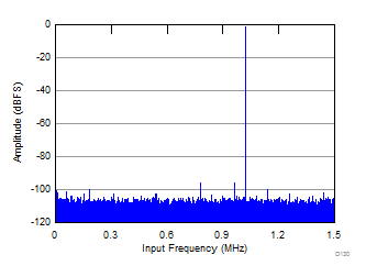
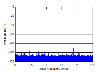
ADS412x, 12-Bit Resolution, at 25°C, AVDD = 1.8 V, DRVDD = 1.8 V, sine wave input clock, 1.5-VPP differential clock amplitude, 50% clock duty cycle, –1-dBFS differential analog input, 0-dB gain, low-latency mode, CMOS output interface, and 32k-point FFT, unless otherwise noted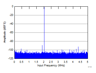
| fS = 10 MSPS, fIN = 12 MHz, SNR = 70.9 dBFS, SFDR = 88 dBc, SINAD = 70.8 dBFS, THD = 86 dBc |
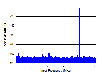 Figure 120. FFT for 20-MSPS Sampling Speed
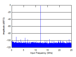 Figure 122. FFT for 50-MSPS Sampling Speed
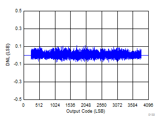
| fS = 3 MSPS, fIN = 4 MHz |
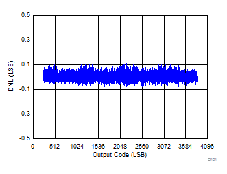
| fS = 5 MSPS, fIN = 3 MHz |
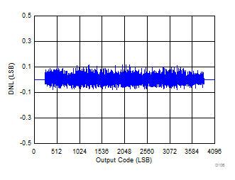
| fS = 10 MSPS, fIN = 3 MHz |
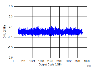
| fS = 20 MSPS, fIN = 3 MHz |
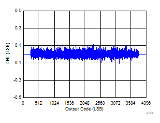
| fS = 50 MSPS, fIN = 3 MHz |
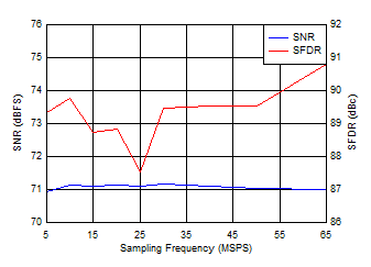
| fIN = 3 MHz |
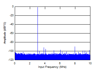 Figure 119. FFT for 20-MSPS Sampling Speed
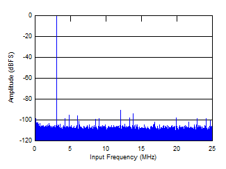 Figure 121. FFT for 50-MSPS Sampling Speed
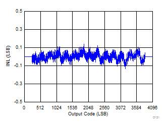
| fS = 3 MSPS, fIN = 4 MHz |
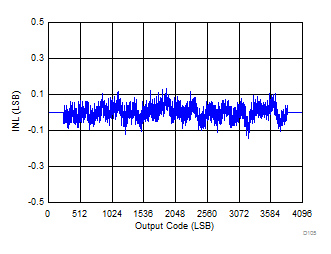
| fS = 10 MSPS, fIN = 3 MHz |
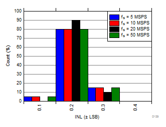
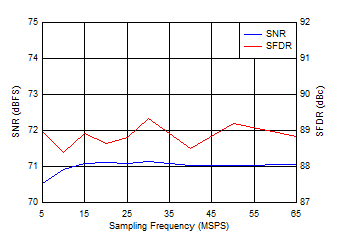
| fIN = 12 MHz |
9.1.4.2 ADS414x (14-Bit Device)
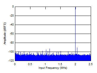
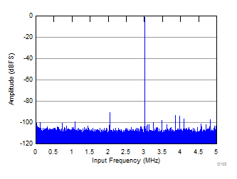
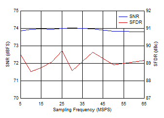
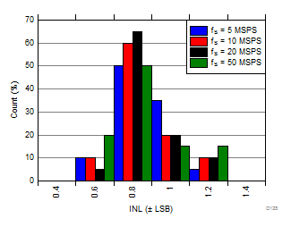
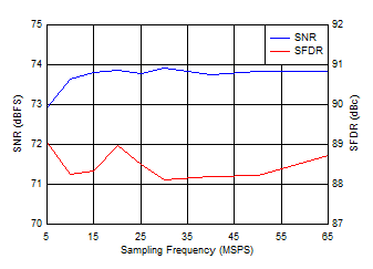
ADS414x, 14-Bit Resolution, at 25°C, AVDD = 1.8 V, DRVDD = 1.8 V, sine wave input clock, 1.5-VPP differential clock amplitude, 50% clock duty cycle, –1-dBFS differential analog input, 0-dB gain, low-latency mode, CMOS output interface, and 32k-point FFT, unless otherwise noted.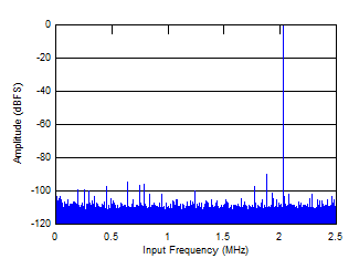 Figure 138. FFT for 5-MSPS Sampling Speed
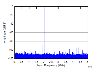
| fS = 10 MSPS, fIN = 12 MHz, SNR = 73.6 dBFS, SFDR = 88 dBc, SINAD = 73.4 dBFS, THD = 86 dBc |
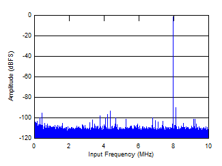
| fS = 20 MSPS, fIN = 12 MHz, SNR = 73.9 dBFS, SFDR = 89 dBc, SINAD = 73.7 dBFS, THD = 87 dBc |
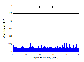
| fS = 50 MSPS, fIN = 12 MHz, SNR = 73.8 dBFS, SFDR = 88 dBc, SINAD = 73.6 dBFS, THD = 86 dBc |
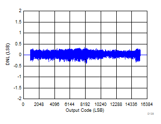
| fS = 3 MSPS, fIN = 4 MHz |
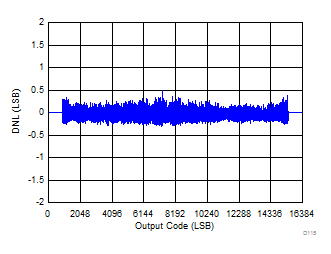
| fS = 5 MSPS, fIN = 3 MHz |
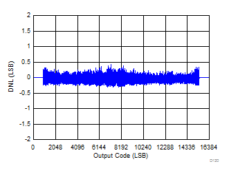
| fS = 10 MSPS, fIN = 3 MHz |
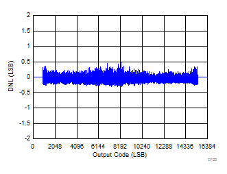
| fS = 20 MSPS, fIN = 3 MHz |

| fS = 50 MSPS, fIN = 3 MHz |
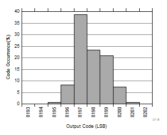
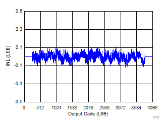
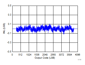
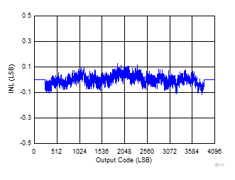
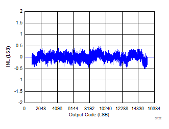
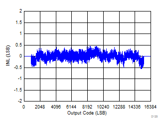
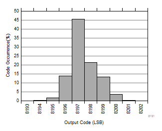
| RMS = 1.1523 LSB |
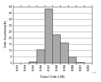
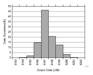
| RMS = 1.104 LSB |
| fIN = 3 MHz |
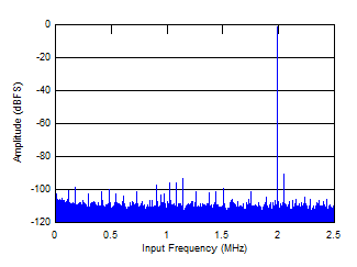 Figure 137. FFT for 5-MSPS Sampling Speed
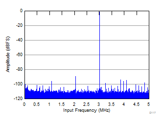
| fS = 10 MSPS, fIN = 3 MHz, SNR = 73.9 dBFS, SFDR = 88 dBc, SINAD = 73.7 dBFS, THD = 86 dBc |
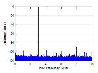 Figure 141. FFT for 20-MSPS Sampling Speed
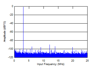
| fS = 50 MSPS, fIN = 3 MHz, SNR = 73.8 dBFS, SFDR = 89 dBc, SINAD = 73.6 dBFS, THD = 86 dBc |
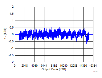
| fS = 3 MSPS, fIN = 4 MHz |
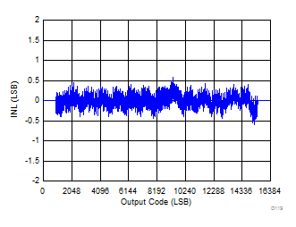
| fS = 10 MSPS, fIN = 3 MHz |
| RMS = 1.080 LSB |
| RMS = 1.072 LSB |
| fIN = 12 MHz |
9.1.4.3 Power Consumption at Low Sampling Rates
Figure 162 shows typical power consumption at lower sampling rates on each supply.
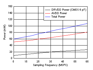 Figure 162. Power vs Sample Rate
9.1.4.4 Output Timing at Low Sampling Rates
Table 9 describes the set-up and hold times for the digital outputs of the ADS41xx with respect to the output clock at low sampling rates.
Table 9. Output Timing at Low Sampling Rates in CMOS Mode(1)
| SAMPLING FREQUENCY (MSPS) | SETUP TIME, tSU | HOLD TIME, tHO | UNIT | ||||
|---|---|---|---|---|---|---|---|
| MIN | TYP | MAX | MIN | TYP | MAX | ||
| CMOS (Low Latency Enabled) | |||||||
| 5 | 99.4 | 100.4 | 97.9 | 98.7 | ns | ||
| 10 | 49.0 | 49.7 | 48.5 | 49.3 | ns | ||
| 20 | 23.3 | 24.2 | 23.9 | 24.8 | ns | ||
| 30 | 15.0 | 15.8 | 15.7 | 16.6 | ns | ||
| 40 | 10.7 | 11.4 | 11.5 | 12.5 | ns | ||
| 50 | 8.2 | 9.0 | 9.1 | 10.0 | ns | ||
| CMOS (Low Latency Disabled) | |||||||
| 5 | 99.6 | 100.3 | 97.8 | 98.5 | ns | ||
| 10 | 49.1 | 49.7 | 48.2 | 49.1 | ns | ||
| 20 | 23.6 | 24.2 | 23.6 | 24.6 | ns | ||
| 30 | 15.2 | 15.7 | 15.3 | 16.4 | ns | ||
| 40 | 10.9 | 11.4 | 11.2 | 12.3 | ns | ||
| 50 | 8.4 | 8.9 | 8.6 | 9.8 | ns | ||
9.2 Typical Application
An example schematic for a typical application of the ADS414x is shown in Figure 163.
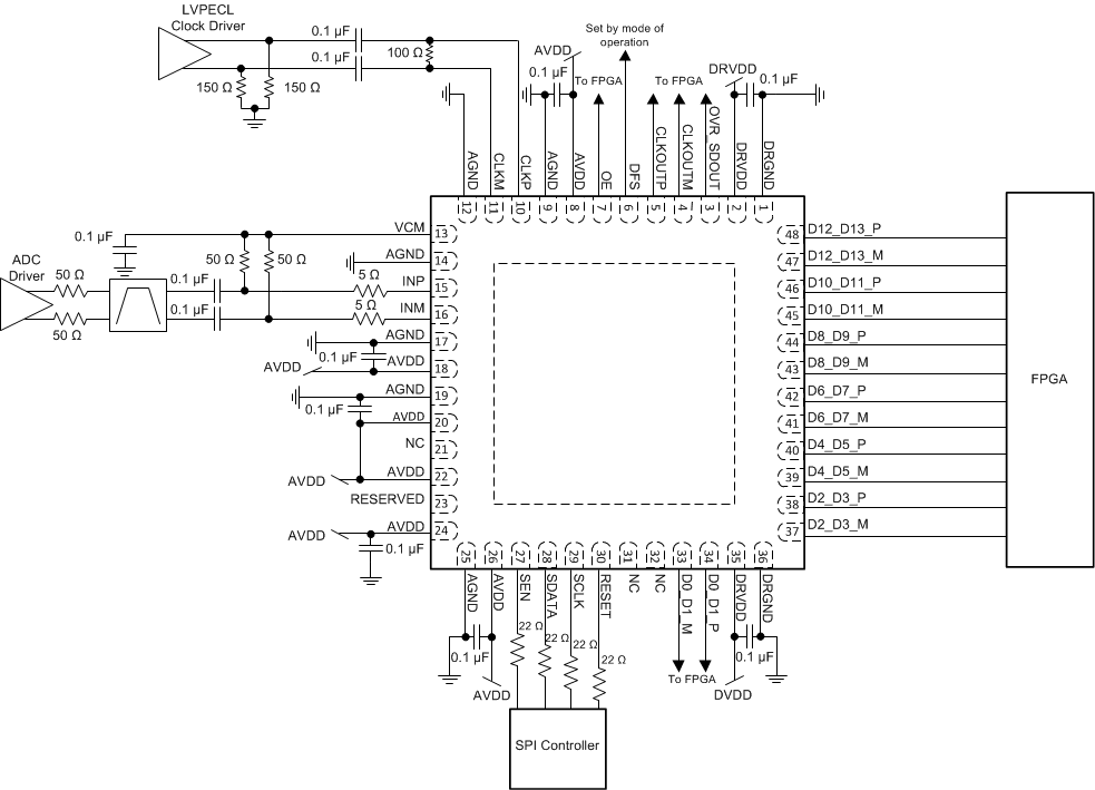 Figure 163. Example Schematic for the ADS414x
9.2.1 Design Requirements
Example design requirements are listed in Table 10 for the ADC portion of the signal chain. These requirements do not necessary reflect the requirements of an actual system, but rather demonstrate why the ADS412x and ADS414x can be chosen for a system based on a set of requirements.
Table 10. Example Design Requirements for the ADS412x and ADS414x
9.2.2 Detailed Design Procedure
9.2.2.1 Analog Input
The analog input of the ADS412x and ADS414x is typically driven by a fully differential amplifier. The amplifier must have sufficient bandwidth for the frequencies of interest. The noise and distortion performance of the amplifier affect the combined performance of the ADC and amplifier. The amplifier is often ac-coupled to the ADC to allow both the amplifier and ADC to operate at the optimal common-mode voltages. The amplifier can be dc-coupled to the ADC if required. An alternate approach is to drive the ADC using transformers. DC coupling cannot be used with the transformer approach.
9.2.2.2 Clock Driver
The ADS412x and ADS414x must be driven by a high-performance clock driver such as a clock jitter cleaner. The clock must have low noise to maintain optimal performance. LVPECL is the most common clocking interface, but LVDS and LVCMOS can be used as well. TI does not advise driving the clock input from an FPGA unless the noise degradation can be tolerated, such as for input signals near dc where the clock noise impact is minimal.
9.2.2.3 Digital Interface
The ADS412x and ADS414x supports both LVDS and CMOS interfaces. The LVDS interface must be used for best performance when operating at maximum sampling rate. The LVDS outputs can be connected directly to the FPGA without any additional components. When using CMOS outputs resistors must be placed in series with the outputs to reduce the output current spikes to limit the performance degradation. The resistors must be large enough to limit current spikes but not so large as to significantly distort the digital output waveform. An external CMOS buffer must be used when driving distances greater than a few inches to reduce ground bounce within the ADC.
9.2.3 Application Curve
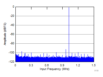
Figure 164 shows the results of a 100-MHz signal sampled at 65 MHz captured by the ADS4122.
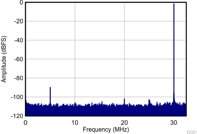
| SNR = 70.11 dBFS, SFDR = 87.74 dBFS, THD = 84.33 dB, SINAD = 70.03 dBFS |
