SBAS569B May   2013  – February 2019 ADS8860

PRODUCTION DATA.  

  1. Features
  2. Applications
  3. Description
    1.     Device Images
      1.      No Separate LDO Required for the ADC Supply
  4. Revision History
  5. Device Comparison Table
  6. Pin Configuration and Functions
    1.     Pin Functions
  7. Specifications
    1. 7.1 Absolute Maximum Ratings
    2. 7.2 ESD Ratings
    3. 7.3 Recommended Operating Conditions
    4. 7.4 Thermal Information
    5. 7.5 Electrical Characteristics
    6. 7.6 Timing Requirements: 3-Wire Operation
    7. 7.7 Timing Requirements: 4-Wire Operation
    8. 7.8 Timing Requirements: Daisy-Chain
    9. 7.9 Typical Characteristics
  8. Parameter Measurement Information
    1. 8.1 Equivalent Circuits
  9. Detailed Description
    1. 9.1 Overview
    2. 9.2 Functional Block Diagram
    3. 9.3 Feature Description
      1. 9.3.1 Analog Input
      2. 9.3.2 Reference
      3. 9.3.3 Clock
      4. 9.3.4 ADC Transfer Function
    4. 9.4 Device Functional Modes
      1. 9.4.1 CS Mode
        1. 9.4.1.1 3-Wire CS Mode Without a Busy Indicator
        2. 9.4.1.2 3-Wire CS Mode With a Busy Indicator
        3. 9.4.1.3 4-Wire CS Mode Without a Busy Indicator
        4. 9.4.1.4 4-Wire CS Mode With a Busy Indicator
      2. 9.4.2 Daisy-Chain Mode
        1. 9.4.2.1 Daisy-Chain Mode Without a Busy Indicator
        2. 9.4.2.2 Daisy-Chain Mode With a Busy Indicator
  10. 10Application and Implementation
    1. 10.1 Application Information
      1. 10.1.1 ADC Reference Driver
      2. 10.1.2 ADC Input Driver
        1. 10.1.2.1 Input Amplifier Selection
        2. 10.1.2.2 Charge-Kickback Filter
    2. 10.2 Typical Applications
      1. 10.2.1 DAQ Circuit for a 1-µs, Full-Scale Step Response
        1. 10.2.1.1 Design Requirements
        2. 10.2.1.2 Detailed Design Procedure
      2. 10.2.2 DAQ Circuit for Lowest Distortion and Noise Performance at 1 MSPS
        1. 10.2.2.1 Design Requirements
        2. 10.2.2.2 Detailed Design Procedure
      3. 10.2.3 Ultralow-Power DAQ Circuit at 10 kSPS
        1. 10.2.3.1 Design Requirements
        2. 10.2.3.2 Detailed Design Procedure
  11. 11Power Supply Recommendations
    1. 11.1 Power-Supply Decoupling
    2. 11.2 Power Saving
  12. 12Layout
    1. 12.1 Layout Guidelines
    2. 12.2 Layout Example
  13. 13Device and Documentation Support
    1. 13.1 Documentation Support
      1. 13.1.1 Related Documentation
    2. 13.2 Receiving Notification of Documentation Updates
    3. 13.3 Community Resources
    4. 13.4 Trademarks
    5. 13.5 Electrostatic Discharge Caution
    6. 13.6 Glossary
  14. 14Mechanical, Packaging, and Orderable Information

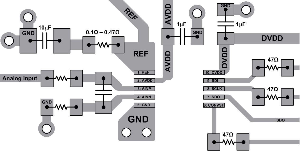
Layout Example

ADS8860 ADS88xx_se_LAYOUT.gifFigure 69. Recommended Layout