SBAS815A
February 2017 – June 2017
ADS114S06
,
ADS114S08
PRODUCTION DATA.
1
Features
2
Applications
3
Description
Device Images
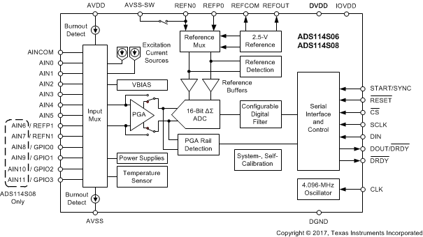
Functional Block Diagram
4
Revision History
5
Device Family Comparison Table
6
Pin Configuration and Functions
Pin Functions
7
Specifications
7.1
Absolute Maximum Ratings
7.2
ESD Ratings
7.3
Recommended Operating Conditions
7.4
Thermal Information
7.5
Electrical Characteristics
7.6
Timing Characteristics
7.7
Switching Characteristics
7.8
Typical Characteristics
8
Parameter Measurement Information
8.1
Noise Performance
9
Detailed Description
9.1
Overview
9.2
Functional Block Diagram
9.3
Feature Description
9.3.1
Multiplexer
9.3.2
Low-Noise Programmable Gain Amplifier
9.3.2.1
PGA Input-Voltage Requirements
9.3.2.2
PGA Rail Flags
9.3.2.3
Bypassing the PGA
9.3.3
Voltage Reference
9.3.3.1
Internal Reference
9.3.3.2
External Reference
9.3.3.3
Reference Buffers
9.3.4
Clock Source
9.3.5
Delta-Sigma Modulator
9.3.6
Digital Filter
9.3.6.1
Low-Latency Filter
9.3.6.1.1
Low-Latency Filter Frequency Response
9.3.6.1.2
Data Conversion Time for the Low-Latency Filter
9.3.6.2
Sinc3 Filter
9.3.6.2.1
Sinc3 Filter Frequency Response
9.3.6.2.2
Data Conversion Time for the Sinc3 Filter
9.3.6.3
Note on Conversion Time
9.3.6.4
50-Hz and 60-Hz Line Cycle Rejection
9.3.6.5
Global Chop Mode
9.3.7
Excitation Current Sources (IDACs)
9.3.8
Bias Voltage Generation
9.3.9
System Monitor
9.3.9.1
Internal Temperature Sensor
9.3.9.2
Power Supply Monitors
9.3.9.3
Burn-Out Current Sources
9.3.10
Status Register
9.3.10.1
POR Flag
9.3.10.2
RDY Flag
9.3.10.3
PGA Output Voltage Rail Monitors
9.3.10.4
Reference Monitor
9.3.11
General-Purpose Inputs and Outputs (GPIOs)
9.3.12
Low-Side Power Switch
9.3.13
Cyclic Redundancy Check (CRC)
9.3.14
Calibration
9.3.14.1
Offset Calibration
9.3.14.2
Gain Calibration
9.4
Device Functional Modes
9.4.1
Reset
9.4.1.1
Power-On Reset
9.4.1.2
RESET Pin
9.4.1.3
Reset by Command
9.4.2
Power-Down Mode
9.4.3
Standby Mode
9.4.4
Conversion Modes
9.4.4.1
Continuous Conversion Mode
9.4.4.2
Single-Shot Conversion Mode
9.4.4.3
Programmable Conversion Delay
9.5
Programming
9.5.1
Serial Interface
9.5.1.1
Chip Select (CS)
9.5.1.2
Serial Clock (SCLK)
9.5.1.3
Serial Data Input (DIN)
9.5.1.4
Serial Data Output and Data Ready (DOUT/DRDY)
9.5.1.5
Data Ready (DRDY)
9.5.1.6
Timeout
9.5.2
Data Format
9.5.3
Commands
9.5.3.1
NOP
9.5.3.2
WAKEUP
9.5.3.3
POWERDOWN
9.5.3.4
RESET
9.5.3.5
START
9.5.3.6
STOP
9.5.3.7
SYOCAL
9.5.3.8
SYGCAL
9.5.3.9
SFOCAL
9.5.3.10
RDATA
9.5.3.11
RREG
9.5.3.12
WREG
9.5.4
Reading Data
9.5.4.1
Read Data Direct
9.5.4.2
Read Data by RDATA Command
9.5.4.3
Sending Commands When Reading Data
9.5.5
Interfacing with Multiple Devices
9.6
Register Map
9.6.1
Configuration Registers
9.6.1.1
Device ID Register (address = 00h) [reset = xxh]
Table 26.
Device ID (ID) Register Field Descriptions
9.6.1.2
Device Status Register (address = 01h) [reset = 80h]
Table 27.
Device Status (STATUS) Register Field Descriptions
9.6.1.3
Input Multiplexer Register (address = 02h) [reset = 01h]
Table 28.
Input Multiplexer (INPMUX) Register Field Descriptions
9.6.1.4
Gain Setting Register (address = 03h) [reset = 00h]
Table 29.
Gain Setting (PGA) Register Field Descriptions
9.6.1.5
Data Rate Register (address = 04h) [reset = 14h]
Table 30.
Data Rate (DATARATE) Register Field Descriptions
9.6.1.6
Reference Control Register (address = 05h) [reset = 10h]
Table 31.
Reference Control (REF) Register Field Descriptions
9.6.1.7
Excitation Current Register 1 (address = 06h) [reset = 00h]
Table 32.
Excitation Current Register 1 (IDACMAG) Register Field Descriptions
9.6.1.8
Excitation Current Register 2 (address = 07h) [reset = FFh]
Table 33.
Excitation Current Register 2 (IDACMUX) Register Field Descriptions
9.6.1.9
Sensor Biasing Register (address = 08h) [reset = 00h]
Table 34.
Sensor Biasing (VBIAS) Register Field Descriptions
9.6.1.10
System Control Register (address = 09h) [reset = 10h]
Table 35.
System Control (SYS) Register Field Descriptions
9.6.1.11
Reserved Register (address = 0Ah) [reset = 00h]
Table 36.
Reserved Register Field Descriptions
9.6.1.12
Offset Calibration Register 1 (address = 0Bh) [reset = 00h]
Table 37.
Offset Calibration Register 1 (OFCAL0) Register Field Descriptions
9.6.1.13
Offset Calibration Register 2 (address = 0Ch) [reset = 00h]
Table 38.
Offset Calibration Register 2 (OFCAL1) Register Field Descriptions
9.6.1.14
Reserved Register (address = 0Dh) [reset = 00h]
Table 39.
Reserved Register Field Descriptions
9.6.1.15
Gain Calibration Register 1 (address = 0Eh) [reset = 00h]
Table 40.
Gain Calibration Register 1 (FSCAL0) Field Descriptions
9.6.1.16
Gain Calibration Register 2 (address = 0Fh) [reset = 40h]
Table 41.
Gain Calibration Register 2 (FSCAL1) Field Descriptions
9.6.1.17
GPIO Data Register (address = 10h) [reset = 00h]
Table 42.
GPIO Data (GPIODAT) Register Field Descriptions
9.6.1.18
GPIO Configuration Register (address = 11h) [reset = 00h]
Table 43.
GPIO Configuration (GPIOCON) Register Field Descriptions
10
Application and Implementation
10.1
Application Information
10.1.1
Serial Interface Connections
10.1.2
Analog Input Filtering
10.1.3
External Reference and Ratiometric Measurements
10.1.4
Establishing a Proper Input Voltage
10.1.5
Unused Inputs and Outputs
10.1.6
Pseudo Code Example
10.2
Typical Application
10.2.1
Design Requirements
10.2.2
Detailed Design Procedure
10.2.2.1
Register Settings
10.2.3
Application Curves
10.3
Do's and Don'ts
11
Power Supply Recommendations
11.1
Power Supplies
11.2
Power-Supply Sequencing
11.3
Power-On Reset
11.4
Power-Supply Decoupling
12
Layout
12.1
Layout Guidelines
12.2
Layout Example
13
Device and Documentation Support
13.1
Device Support
13.1.1
Development Support
13.2
Documentation Support
13.2.1
Related Documentation
13.3
Related Links
13.4
Receiving Notification of Documentation Updates
13.5
Community Resources
13.6
Trademarks
13.7
Electrostatic Discharge Caution
13.8
Glossary
14
Mechanical, Packaging, and Orderable Information
9.2
Functional Block Diagram