SBAS817D November 2017 – June 2024 ADS8166 , ADS8167 , ADS8168
PRODUCTION DATA
- 1
- 1 Features
- 2 Applications
- 3 Description
- 4 Pin Configuration and Functions
- 5 Specifications
- 6 Detailed Description
-
7 Register Maps
- 7.1
Interface and Hardware Configuration Registers
- 7.1.1 REG_ACCESS Register (address = 00h) [reset = 00h]
- 7.1.2 PD_CNTL Register (address = 04h) [reset = 00h]
- 7.1.3 SDI_CNTL Register (address = 008h) [reset = 00h]
- 7.1.4 SDO_CNTL1 Register (address = 0Ch) [reset = 00h]
- 7.1.5 SDO_CNTL2 Register (address = 0Dh) [reset = 00h]
- 7.1.6 SDO_CNTL3 Register (address = 0Eh) [reset = 00h]
- 7.1.7 SDO_CNTL4 Register (address = 0Fh) [reset = 00h]
- 7.1.8 DATA_CNTL Register (address = 10h) [reset = 00h]
- 7.1.9 PARITY_CNTL Register (address = 11h) [reset = 00h]
- 7.2 Device Calibration Registers
- 7.3 Analog Input Configuration Registers
- 7.4
Channel Sequence Configuration Registers Map
- 7.4.1 DEVICE_CFG Register (address = 1Ch) [reset = 00h]
- 7.4.2 CHANNEL_ID Register (address = 1Dh) [reset = 00h]
- 7.4.3 SEQ_START Register (address = 1Eh) [reset = 00h]
- 7.4.4 SEQ_ABORT Register (address = 1Fh) [reset = 00h]
- 7.4.5 ON_THE_FLY_CFG Register (address = 2Ah) [reset = 00h]
- 7.4.6 AUTO_SEQ_CFG1 Register (address = 80h) [reset = 00h]
- 7.4.7 AUTO_SEQ_CFG2 Register (address = 82h) [reset = 00h]
- 7.4.8
Custom Channel Sequencing Mode Registers
- 7.4.8.1 CCS_START_INDEX Register (address = 88h) [reset = 00h]
- 7.4.8.2 CCS_END_INDEX Register (address = 89h) [reset = 00h]
- 7.4.8.3 CCS_SEQ_LOOP Register (address = 8Ah) [reset = 00h]
- 7.4.8.4 CCS_CHID_INDEX_m Registers (address = 8C, 8E, 90, 92, 94, 96, 98, 9A, 9C, 9E, A0, A2, A4, A6, A8, and AAh) [reset = 00h]
- 7.4.8.5 REPEAT_INDEX_m Registers (address = 8D, 8F, 91, 93, 95, 97, 99, 9B, 9D, 9F, A1, A3, A5, A7, A9, and ABh) [reset = 00h]
- 7.5
Digital Window Comparator Configuration Registers Map
- 7.5.1 ALERT_CFG Register (address = 2Eh) [reset = 00h]
- 7.5.2 HI_TRIG_AINx[15:0] Register (address = 4Dh to 30h) [reset = 0000h]
- 7.5.3 LO_TRIG_AINx[15:0] Register (address = 71h to 54h) [reset = 0000h]
- 7.5.4 HYSTERESIS_AINx[7:0] Register (address = 4Fh to 33h) [reset = 00h]
- 7.5.5 ALERT_LO_STATUS Register (address = 78h) [reset = 00h]
- 7.5.6 ALERT_HI_STATUS Register (address = 79h) [reset = 00h]
- 7.5.7 ALERT_STATUS Register (address = 7Ah) [reset = 00h]
- 7.5.8 CURR_ALERT_LO_STATUS Register (address = 7Ch) [reset = 00h]
- 7.5.9 CURR_ALERT_HI_STATUS Register (address = 7Dh) [reset = 00h]
- 7.5.10 CURR_ALERT_STATUS Register (address = 7Eh) [reset = 00h]
- 7.1
Interface and Hardware Configuration Registers
- 8 Application and Implementation
- 9 Device and Documentation Support
- 10Revision History
- 11Mechanical, Packaging, and Orderable Information
6.5.2 Register Read/Write Operation
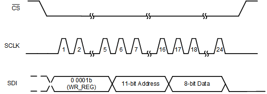
This device features configuration registers (as described in the Interface and Hardware Configuration Registers section). These devices support the commands listed in Table 6-8 to access the internal configuration registers.
| B[23:19] | B[18:8] | B[7:0] | COMMAND ACRONYM | COMMAND DESCRIPTION |
|---|---|---|---|---|
| 00000 | 00000000000 | 00000000 | NOP | No operation |
| 00001 | <11-bit address> | <8-bit data> | WR_REG | Write <8-bit data> to the <11-bit address> |
| 00010 | <11-bit address> | 00000000 | RD_REG | Read contents from the <11-bit address> |
| 00011 | <11-bit address> | <8-bit unmasked bits> | SET_BITS | Set <8-bit unmasked bits> from <11-bit address> |
| 00100 | <11-bit address> | <8-bit unmasked bits> | CLR_BITS | Clear <8-bit unmasked bits> from <11-bit address> |
| Remaining combinations | xxxxxxxxx | xxxxxxxx | Reserved | These commands are reserved and treated by the device as no operation |
The ADS816x supports two types of data transfer operations: data write (the host controller configures the device), and data read (the host controller reads data from the device).
Any data write to the device is always synchronous to the external clock provided on the SCLK pin. The WR_REG command writes the 8-bit data into the 11-bit address specified in the command string. The CLR_BITS command clears the specified bits (identified by 1) at the 11-bit address (without affecting the other bits), and the SET_BITS command sets the specified bits (identified by 1) at the 11-bit address (without affecting the other bits).
Figure 6-25 shows the digital waveform for register read operation. Register read operation consists of two frames: one frame to initiate a register read and a second frame to read data from the register address provided in the first frame. As shown in Figure 6-25, the 11-bit register address and the 8-bit dummy data are sent over the SDI pin during the first 24-bit frame with the read command (00010b). When CS goes from low to high, this read command is decoded and the requested register data are available for reading during the next frame. During the second frame, the first eight bits on SDO correspond to the requested register read. During the second frame, use SDI to initiate another operation or set SDI to 0.
 Figure 6-25 Register Read Operation
Figure 6-26 shows that for writing data to the register, one 24-bit frame is required. The 24-bit data on SDI consists of a 5-bit write command (00001b), an 11-bit register address, and 8-bit data. The write command is decoded on the CS rising edge and the specified register is updated with the 8-bit data specified during register write operation.
 Figure 6-26 Register Write Operation