SBAS821 December   2017 ADS7057

PRODUCTION DATA.  

  1. Features
  2. Applications
  3. Description
  4. Revision History
  5. Pin Configuration and Functions
  6. Specifications
    1. 6.1 Absolute Maximum Ratings
    2. 6.2 ESD Ratings
    3. 6.3 Recommended Operating Conditions
    4. 6.4 Thermal Information
    5. 6.5 Electrical Characteristics
    6. 6.6 Timing Requirements
    7. 6.7 Switching Characteristics
    8. 6.8 Typical Characteristics
  7. Parameter Measurement Information
    1. 7.1 Digital Voltage Levels
  8. Detailed Description
    1. 8.1 Overview
    2. 8.2 Functional Block Diagram
    3. 8.3 Feature Description
      1. 8.3.1 Product Family
      2. 8.3.2 Analog Input
      3. 8.3.3 Reference
      4. 8.3.4 ADC Transfer Function
    4. 8.4 Device Functional Modes
      1. 8.4.1 ACQ State
      2. 8.4.2 CNV State
      3. 8.4.3 OFFCAL State
        1. 8.4.3.1 Offset Calibration on Power-Up
        2. 8.4.3.2 Offset Calibration During Normal Operation
  9. Application and Implementation
    1. 9.1 Application Information
    2. 9.2 Typical Applications
      1. 9.2.1 2-Channel, Simultaneous Sampling Data Acquisition Using the ADS7057
        1. 9.2.1.1 Design Requirements
        2. 9.2.1.2 Detailed Design Procedure
          1. 9.2.1.2.1 Low Distortion Charge Kickback Filter Design
          2. 9.2.1.2.2 Input Amplifier Selection
          3. 9.2.1.2.3 Reference Circuit
        3. 9.2.1.3 Application Curves
      2. 9.2.2 Improving Precision of Single-Ended Signal Source Measurements Using the ADS7057
        1. 9.2.2.1 Design Requirements
        2. 9.2.2.2 Detailed Design Procedure
        3. 9.2.2.3 Application Curve
  10. 10Power Supply Recommendations
    1. 10.1 AVDD and DVDD Supply Recommendations
    2. 10.2 Optimizing Power Consumed by the Device
      1. 10.2.1 Estimating Digital Power Consumption
  11. 11Layout
    1. 11.1 Layout Guidelines
    2. 11.2 Layout Example
  12. 12Device and Documentation Support
    1. 12.1 Device Support
      1. 12.1.1 Development Support
    2. 12.2 Documentation Support
      1. 12.2.1 Related Documentation
    3. 12.3 Receiving Notification of Documentation Updates
    4. 12.4 Community Resources
    5. 12.5 Trademarks
    6. 12.6 Electrostatic Discharge Caution
    7. 12.7 Glossary
  13. 13Mechanical, Packaging, and Orderable Information

Parameter Measurement Information

Digital Voltage Levels

The device complies with the JESD8-7A standard for DVDD from 1.65 V to 1.95 V. Figure 32 shows voltage levels for the digital input and output pins.
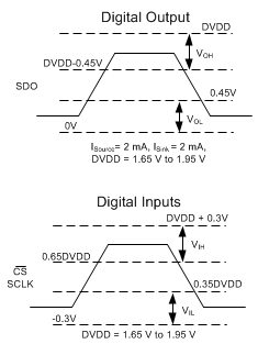
ADS7057 tim_level_bas608.gif Figure 32. Digital Voltage Levels as per the JESD8-7A Standard