SBAS838A January   2018  – October 2018 ADS112U04

PRODUCTION DATA.  

  1. Features
  2. Applications
  3. Description
    1.     Device Images
      1.      K-Type Thermocouple Measurement
  4. Revision History
  5. Pin Configuration and Functions
    1.     Pin Functions
  6. Specifications
    1. 6.1 Absolute Maximum Ratings
    2. 6.2 ESD Ratings
    3. 6.3 Recommended Operating Conditions
    4. 6.4 Thermal Information
    5. 6.5 Electrical Characteristics
    6. 6.6 UART Timing Requirements
    7. 6.7 UART Switching Characteristics
    8. 6.8 Typical Characteristics
  7. Parameter Measurement Information
    1. 7.1 Noise Performance
  8. Detailed Description
    1. 8.1 Overview
    2. 8.2 Functional Block Diagram
    3. 8.3 Feature Description
      1. 8.3.1  Multiplexer
      2. 8.3.2  Low-Noise Programmable Gain Stage
        1. 8.3.2.1 PGA Input Voltage Requirements
        2. 8.3.2.2 Bypassing the PGA
      3. 8.3.3  Voltage Reference
      4. 8.3.4  Modulator and Internal Oscillator
      5. 8.3.5  Digital Filter
      6. 8.3.6  Conversion Times
      7. 8.3.7  Excitation Current Sources
      8. 8.3.8  Sensor Detection
      9. 8.3.9  System Monitor
      10. 8.3.10 Temperature Sensor
        1. 8.3.10.1 Converting From Temperature to Digital Codes
          1. 8.3.10.1.1 For Positive Temperatures (For Example, 50°C):
          2. 8.3.10.1.2 For Negative Temperatures (For Example, –25°C):
        2. 8.3.10.2 Converting From Digital Codes to Temperature
      11. 8.3.11 Offset Calibration
      12. 8.3.12 Conversion Data Counter
      13. 8.3.13 Data Integrity
      14. 8.3.14 General-Purpose Digital Inputs/Outputs
    4. 8.4 Device Functional Modes
      1. 8.4.1 Power-Up and Reset
        1. 8.4.1.1 Power-On Reset
        2. 8.4.1.2 RESET Pin
        3. 8.4.1.3 Reset by Command
      2. 8.4.2 Conversion Modes
        1. 8.4.2.1 Single-Shot Conversion Mode
        2. 8.4.2.2 Continuous Conversion Mode
      3. 8.4.3 Operating Modes
        1. 8.4.3.1 Normal Mode
        2. 8.4.3.2 Turbo Mode
        3. 8.4.3.3 Power-Down Mode
    5. 8.5 Programming
      1. 8.5.1 UART Interface
        1. 8.5.1.1 Receive (RX)
        2. 8.5.1.2 Transmit (TX)
        3. 8.5.1.3 Data Ready (DRDY)
        4. 8.5.1.4 Protocol
        5. 8.5.1.5 Timeout
      2. 8.5.2 Data Format
      3. 8.5.3 Commands
        1. 8.5.3.1 RESET (0000 011x)
        2. 8.5.3.2 START/SYNC (0000 100x)
        3. 8.5.3.3 POWERDOWN (0000 001x)
        4. 8.5.3.4 RDATA (0001 xxxx)
        5. 8.5.3.5 RREG (0010 rrrx)
        6. 8.5.3.6 WREG (0100 rrrx dddd dddd)
        7. 8.5.3.7 Command Latching
      4. 8.5.4 Reading Data
        1. 8.5.4.1 Manual Data Read Mode
        2. 8.5.4.2 Automatic Data Read Mode
      5. 8.5.5 Data Integrity
    6. 8.6 Register Map
      1. 8.6.1 Configuration Registers
      2. 8.6.2 Register Descriptions
        1. 8.6.2.1 Configuration Register 0 (address = 00h) [reset = 00h]
          1. Table 18. Configuration Register 0 Field Descriptions
        2. 8.6.2.2 Configuration Register 1 (address = 01h) [reset = 00h]
          1. Table 19. Configuration Register 1 Field Descriptions
        3. 8.6.2.3 Configuration Register 2 (address = 02h) [reset = 00h]
          1. Table 21. Configuration Register 2 Field Descriptions
        4. 8.6.2.4 Configuration Register 3 (address = 03h) [reset = 00h]
          1. Table 22. Configuration Register 3 Field Descriptions
        5. 8.6.2.5 Configuration Register 4 (address = 04h) [reset = 00h]
          1. Table 23. Configuration Register 4 Field Descriptions
  9. Application and Implementation
    1. 9.1 Application Information
      1. 9.1.1 Interface Connections
      2. 9.1.2 Analog Input Filtering
      3. 9.1.3 External Reference and Ratiometric Measurements
      4. 9.1.4 Establishing Proper Limits on the Absolute Input Voltage
      5. 9.1.5 Unused Inputs and Outputs
      6. 9.1.6 Pseudo Code Example
    2. 9.2 Typical Applications
      1. 9.2.1 K-Type Thermocouple Measurement (–200°C to +1250°C)
        1. 9.2.1.1 Design Requirements
        2. 9.2.1.2 Detailed Design Procedure
        3. 9.2.1.3 Application Curves
      2. 9.2.2 3-Wire RTD Measurement (–200°C to +850°C)
        1. 9.2.2.1 Design Requirements
        2. 9.2.2.2 Detailed Design Procedure
          1. 9.2.2.2.1 Design Variations for 2-Wire and 4-Wire RTD Measurements
        3. 9.2.2.3 Application Curves
      3. 9.2.3 Resistive Bridge Measurement
        1. 9.2.3.1 Design Requirements
        2. 9.2.3.2 Detailed Design Procedure
  10. 10Power Supply Recommendations
    1. 10.1 Power-Supply Sequencing
    2. 10.2 Power-Supply Decoupling
  11. 11Layout
    1. 11.1 Layout Guidelines
    2. 11.2 Layout Example
  12. 12Device and Documentation Support
    1. 12.1 Documentation Support
      1. 12.1.1 Related Documentation
    2. 12.2 Receiving Notification of Documentation Updates
    3. 12.3 Community Resources
    4. 12.4 Trademarks
    5. 12.5 Electrostatic Discharge Caution
    6. 12.6 Glossary
  13. 13Mechanical, Packaging, and Orderable Information

Digital Filter

The device uses a linear-phase finite impulse response (FIR) digital filter that performs both filtering and decimation of the digital data stream coming from the modulator. The digital filter is automatically adjusted for the different data rates and always settles within a single cycle. The frequency responses of the digital filter are illustrated in Figure 48 to Figure 56 for different output data rates. The filter notches and output data rate scale proportionally with the clock frequency. The internal oscillator can vary over temperature as specified in the Electrical Characteristics table. The data rate or conversion time, respectively, and consequently also the filter notches vary proportionally.
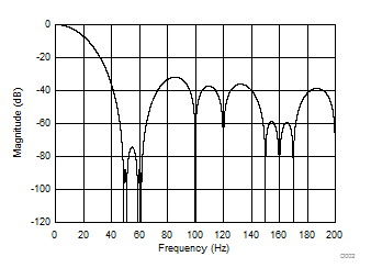
ADS112U04 D002.gifFigure 48. Filter Response
(Normal Mode, DR = 20 SPS)
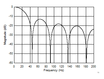
ADS112U04 filt_45SPS.gifFigure 50. Filter Response
(Normal Mode, DR = 45 SPS)
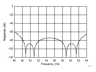
ADS112U04 D001.gifFigure 49. Detailed View of the Filter Response
(Normal Mode, DR = 20 SPS)
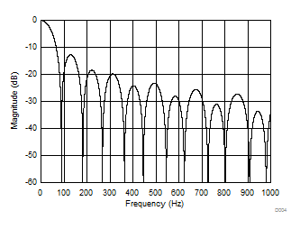
ADS112U04 D004.gifFigure 51. Filter Response
(Normal Mode, DR = 90 SPS)
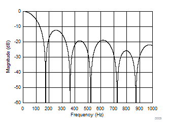
ADS112U04 D005.gifFigure 52. Filter Response
(Normal Mode, DR = 175 SPS)
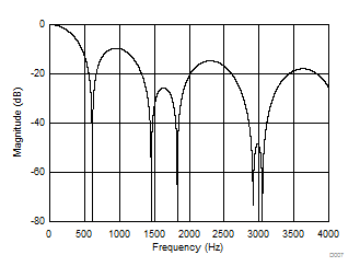
ADS112U04 D007_sbas751.gifFigure 54. Filter Response
(Normal Mode, DR = 600 SPS)
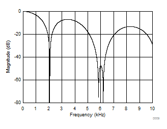
ADS112U04 D009_sbas751.gifFigure 56. Filter Response
(Turbo Mode, DR = 2 kSPS)
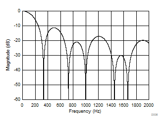
ADS112U04 D006.gifFigure 53. Filter Response
(Normal Mode, DR = 330 SPS)
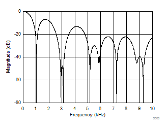
ADS112U04 D008_sbas751.gifFigure 55. Filter Response
(Normal Mode, DR = 1 kSPS)