SBAS846 November 2017 TLA2021 , TLA2022 , TLA2024
PRODUCTION DATA.
- 1 Features
- 2 Applications
- 3 Description
- 4 Revision History
- 5 Device Comparison Table
- 6 Pin Configuration and Functions
- 7 Specifications
- 8 Detailed Description
- 9 Register Maps
- 10Application and Implementation
- 11Power Supply Recommendations
- 12Layout
- 13Device and Documentation Support
- 14Mechanical, Packaging, and Orderable Information
12 Layout
12.1 Layout Guidelines
Employ best design practices when laying out a printed-circuit board (PCB) for both analog and digital components. For optimal performance, separate the analog components such as ADCs, amplifiers, references, digital-to-analog converters (DACs), and analog MUXs from digital components such as microcontrollers, complex programmable logic devices (CPLDs), field-programmable gate arrays (FPGAs), radio frequency (RF) transceivers, universal serial bus (USB) transceivers, and switching regulators. Figure 28 shows an example of good component placement. Although Figure 28 provides a good example of component placement, the best placement for each application is unique to the geometries, components, and PCB fabrication capabilities. That is, there is no single layout that is perfect for every design and careful consideration must always be used when designing with any analog component.
 Figure 28. System Component Placement
The following points outline some basic recommendations for the layout of the TLA202x to get the best possible performance of the ADC. A good design can be ruined with a bad circuit layout.
- Separate the analog and digital signals. To start, partition the board into analog and digital sections where the layout permits. Route digital lines away from analog lines to prevent digital noise from coupling back into analog signals.
- Fill void areas on signal layers with ground fill.
- Provide good ground return paths. Signal return currents flow on the path of least impedance. If the ground plane is cut or has other traces that block the current from flowing right next to the signal trace, the ground plane must find another path to return to the source and complete the circuit. If the ground plane is forced into a larger path, there is an increased chance of signal radiation. Sensitive signals are more susceptible to EMI interference.
- Use bypass capacitors on supplies to minimize high-frequency noise. Do not place vias between bypass capacitors and the active device. For best results, place the bypass capacitors on the same layer as close as possible to the active device.
- Consider the resistance and inductance of the routing. Input traces often have resistances that react with the input bias current and cause an added error voltage. Reduce the loop area enclosed by the source signal and the return current to minimize the inductance in the path.
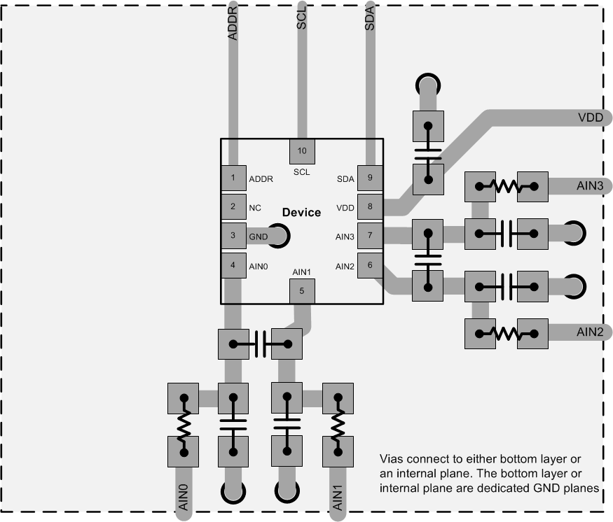
- For best input combinations with differential measurements, use adjacent analog input lines such as AIN0, AIN1 and AIN2, AIN3. The differential capacitors must be of high quality. The best ceramic chip capacitors are C0G (NPO) capacitors, which have stable properties and low-noise characteristics.
12.2 Layout Example
 Figure 29. TLA2024 X2QFN Package