SBAS876C August 2018 – June 2019 ADS9224R , ADS9234R
PRODUCTION DATA.
- 1 Features
- 2 Applications
- 3 Description
- 4 Revision History
- 5 Pin Configuration and Functions
-
6 Specifications
- 6.1 Absolute Maximum Ratings
- 6.2 ESD Ratings
- 6.3 Recommended Operating Conditions
- 6.4 Thermal Information
- 6.5 Electrical Characteristics: ADS92x4R
- 6.6 Electrical Characteristics: ADS9224R
- 6.7 Electrical Characteristics: ADS9234R
- 6.8 Timing Requirements
- 6.9 Switching Characteristics
- 6.10 Typical Characteristics: ADS9224R
- 6.11 Typical Characteristics: ADS9234R
-
7 Detailed Description
- 7.1 Overview
- 7.2 Functional Block Diagram
- 7.3 Feature Description
- 7.4 Device Functional Modes
- 7.5 READY/STROBE Output
- 7.6
Programming
- 7.6.1 Output Data Word
- 7.6.2
Data Transfer Protocols
- 7.6.2.1
Protocols for Reading From the Device
- 7.6.2.1.1 Legacy, SPI-Compatible Protocols (SPI-xy-S-SDR)
- 7.6.2.1.2 SPI-Compatible Protocols With Bus Width Options and Single Data Rate (SPI-xy-D-SDR and SPI-xy-Q-SDR)
- 7.6.2.1.3 SPI-Compatible Protocols With Bus Width Options and Double Data Rate (SPI-x1-S-DDR, SPI-x1-D-DDR, SPI-x1-Q-DDR)
- 7.6.2.1.4 Clock Re-Timer (CRT) Protocols (CRT-S-SDR, CRT-D-SDR, CRT-Q-SDR, CRT-S-DDR, CRT-D-DDR, CRT-Q-DDR)
- 7.6.2.1.5 Parallel Byte Protocols (PB-xy-AB-SDR, PB-xy-AA-SDR)
- 7.6.2.2 Device Setup
- 7.6.2.3 Protocols for Configuring the Device
- 7.6.2.1
Protocols for Reading From the Device
- 7.6.3 Reading and Writing Registers
- 7.7
Register Maps
- 7.7.1
ADS92x4R Registers
- 7.7.1.1 DEVICE_STATUS Register (Offset = 0h) [reset = 0h]
- 7.7.1.2 POWER_DOWN_CFG Register (Offset = 1h) [reset = 0h]
- 7.7.1.3 PROTOCOL_CFG Register (Offset = 2h) [reset = 0h]
- 7.7.1.4 BUS_WIDTH Register (Offset = 3h) [reset = 0h]
- 7.7.1.5 CRT_CFG Register (Offset = 4h) [reset = 0h]
- 7.7.1.6 OUTPUT_DATA_WORD_CFG Register (Offset = 5h) [reset = 0h]
- 7.7.1.7 DATA_AVG_CFG Register (Offset = 6h) [reset = 0h]
- 7.7.1.8 REFBY2_OFFSET Register (Offset = 7h) [reset = 0h]
- 7.7.1
ADS92x4R Registers
- 8 Application and Implementation
- 9 Power Supply Recommendations
- 10Layout
- 11Device and Documentation Support
- 12Mechanical, Packaging, and Orderable Information
8.1.1.1 Charge-Kickback Filter
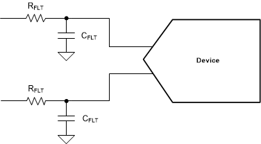
The charge-kickback filter is an RC filter at the input pins of the ADC that filters the broadband noise from the front-end drive circuitry, and attenuates the sampling charge injection from the switched-capacitor input stage of the ADC. A filter capacitor, CFLT (as shown in Figure 79), is connected from each input pin of the ADC to the ground. This capacitor helps reduce the sampling charge injection and provides a charge bucket to quickly charge the internal sample-and-hold capacitors during the acquisition process. Generally, the value of this capacitor must be at least 20 times the specified value of the ADC sampling capacitance. For the ADS92x4R, the input sampling capacitance is equal to 16 pF; therefore, for optimal performance, keep CFLT greater than 320 pF. This capacitor must be a C0G- or NP0-type. The type of dielectric used in C0G or NP0 ceramic capacitors provides the most stable electrical properties over voltage, frequency, and temperature changes.
 Figure 79. Charge Kickback Filter
 Driving capacitive loads can degrade the phase margin of the input amplifier, thus making the amplifier marginally unstable. To avoid amplifier stability issues, series isolation resistors (RFLT) are used at the output of the amplifiers. A higher value of RFLT helps with amplifier stability, but adds distortion as a result of interactions with the nonlinear input impedance of the ADC. Distortion increases with source impedance, input signal frequency, and input signal amplitude. Therefore, the selection of RFLT requires balancing the stability of the driver amplifier and distortion performance of the design. Always verify the stability and settling behavior of the driving amplifier and charge-kickback filter by TINA-TI™ SPICE simulation. Keep the tolerance of the selected resistors less than 1% to keep the inputs balanced.