-
ADC3664 14-Bit, 125-MSPS, Low-Noise, Low Power Dual Channel ADC
- 1 Features
- 2 Applications
- 3 Description
- 4 Revision History
- 5 Pin Configuration and Functions
-
6 Specifications
- 6.1 Absolute Maximum Ratings
- 6.2 ESD Ratings
- 6.3 Recommended Operating Conditions
- 6.4 Thermal Information
- 6.5 Electrical Characteristics - Power Consumption
- 6.6 Electrical Characteristics - DC Specifications
- 6.7 Electrical Characteristics - AC Specifications
- 6.8 Timing Requirements
- 6.9 Typical Characteristics
- 7 Parameter Measurement Information
- 8 Detailed Description
- 9 Application Information Disclaimer
- 10Device and Documentation Support
- 11Mechanical, Packaging, and Orderable Information
- IMPORTANT NOTICE
ADC3664 14-Bit, 125-MSPS, Low-Noise, Low Power Dual Channel ADC
1 Features
- 14-Bit 125 MSPS ADC
- Noise floor: –156.9 dBFS/Hz
- Low power consumption: 100 mW/ch
- Latency: 2 clock cycles
- Voltage reference:
- External: 65 to 125 MSPS
- Internal: 100 to 125 MSPS
- Guaranteed 14-Bit, no missing codes
- Input bandwidth: 1.4 GHz (3 dB)
- INL: ±2.6 LSB; DNL: ±0.9 LSB
- Industrial temperature range: –40°C to +105°C
- On-chip digital filter (optional)
- Decimation by 2, 4, 8, 16, 32
- 32-bit NCO
- Serial LVDS digital interface (2-, 1- and 1/2-wire)
- Small Footprint: 40-VQFN (5 mm × 5 mm) package
- Spectral performance (fIN = 5 MHz):
- SNR: 77.5 dBFS
- SFDR: 84-dBc HD2, HD3
- SFDR: 92-dBFS worst spur
- Spectral performance (fIN = 70 MHz):
- SNR: 75.5 dBFS
- SFDR: 76-dBc HD2, HD3
- SFDR: 84-dBFS worst spur
2 Applications
- High-speed data acquisition
- Software defined radio
- Communications infrastructure
- OTDR
- Control loops
- Source measurement unit (SMU)
- Instrumentation
- Spectroscopy
- Radar
3 Description
The ADC3664 device is a low-noise, ultra-low power, 14-bit, 125-MSPS, high-speed dual channel ADC. Designed for lowest noise performance, the device delivers a noise spectral density of –156.9 dBFS/Hz combined with excellent linearity and dynamic range. The ADC3664 offers IF sampling support which makes the device suited for a wide range of applications. High-speed control loops benefit from the short latency as low as one clock cycle. The ADC consumes only 100 mW/ch at 125 MSPS and its power consumption scales very well with lower sampling rates.
The ADC3664 uses a serial LVDS (SLVDS) interface to output the data which minimizes the number of digital interconnects. The device supports a two-lane, one-lane and half-lane option. The ADC3664 is pin-to-pin compatible with a family of 16-bit resolution ADCs. The device supports the extended industrial temperature range from –40 to +105⁰C.
| PART NUMBER | PACKAGE(1) | BODY SIZE (NOM) |
|---|---|---|
| ADC3664 | VQFN (40) | 5.00 × 5.00 mm |
| PART NUMBER | RESOLUTION | SAMPLING RATE |
|---|---|---|
| ADC3661 | 16 BIT | 10 MSPS |
| ADC3662 | 16 BIT | 25 MSPS |
| ADC3663 | 16 BIT | 65 MSPS |
| ADC3664 | 14 BIT | 125 MSPS |
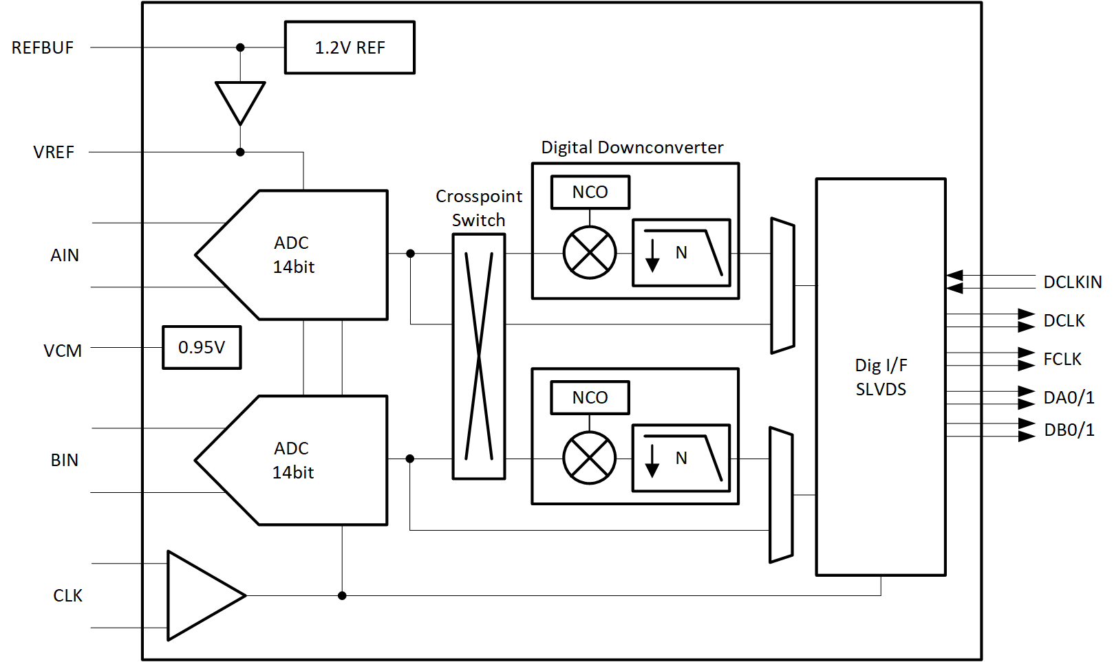
 Simplified Block
Diagram
Simplified Block
Diagram4 Revision History
Changes from Revision A (August 2021) to Revision B (July 2022)
- Changed the output clock jitter unit from ps to ps pk-pk in the Timing RequirementsGo
- Added GND symbol to REFGND pin for all voltage reference option diagramsGo
- Added the section Output Bit Mapper Go
- Added default power up configuration summaryGo
- Updated power-up initialization diagram with correct indexing Go
5 Pin Configuration and Functions
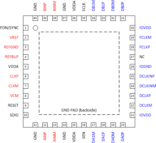
 Figure 5-1 RSB (WQFN) Package, 40-Pin
(Top View)
| PIN | I/O | DESCRIPTION | |
|---|---|---|---|
| NAME | NO. | ||
| INPUT/REFERENCE | |||
| AINM | 13 | I | Negative analog input, channel A |
| AINP | 12 | I | Positive analog input, channel A |
| BINP | 39 | I | Positive analog input, channel B |
| BINM | 38 | I | Negative analog input, channel B |
| REFBUF | 4 | I | 1.2 V external voltage reference input for use with internal reference buffer. Internal 100 kΩ pull-up resistor to AVDD. This pin is also used to configure default operating conditions. |
| REFGND | 3 | I | Reference ground input, 0 V |
| VCM | 8 | O | Common-mode voltage output for the analog inputs, 0.95V |
| VREF | 2 | I | External voltage reference input |
| CLOCK | |||
| CLKM | 7 | I | Negative differential sampling clock input for the ADC |
| CLKP | 6 | I | Positive differential sampling clock input for the ADC |
| CONFIGURATION | |||
| PDN/SYNC | 1 | I | Power down/Synchronization input. This pin can be configured via the SPI interface. Active high. This pin has an internal 21 kΩ pull-down resistor. |
| RESET | 9 | I | Hardware reset. Active high. This pin has an internal 21 kΩ pull-down resistor. |
| SCLK | 35 | I | Serial interface clock input. This pin has an internal 21 kΩ pull-down resistor. |
| SDIO | 10 | I | Serial interface data input and output. This pin has an internal 21 kΩ pull-down resistor. |
| SEN | 16 | I | Serial interface enable. Active low. This pin has an internal 21 kΩ pull-up resistor to AVDD. |
| NC | 27 | - | Do not connect |
| DIGITAL INTERFACE | |||
| DA0P | 20 | O | Positive differential serial LVDS output for lane 0, channel A. |
| DA0M | 19 | O | Negative differential serial LVDS output for lane 0, channel A. |
| DA1P | 18 | O | Positive differential serial LVDS output for lane 1, channel A. |
| DA1M | 17 | O | Negative differential serial LVDS output for lane 1, channel A. |
| DB0P | 31 | O | Positive differential serial LVDS output for lane 0, channel B. |
| DB0M | 32 | O | Negative differential serial LVDS output for lane 0, channel B. |
| DB1P | 33 | O | Positive differential serial LVDS output for lane 1, channel B. |
| DB1M | 34 | O | Negative differential serial LVDS output for lane 1, channel B. |
| DCLKP | 23 | O | Positive differential serial LVDS bit clock output. |
| DCLKM | 22 | O | Negative differential serial LVDS bit clock output. |
| FCLKP | 28 | O | Positive differential serial LVDS frame clock output. |
| FCLKM | 29 | O | Negative differential serial LVDS frame clock output. |
| DCLKINP | 25 | I | Positive differential serial LVDS bit clock input. Internal 100 Ω differential termination. |
| DCLKINM | 24 | I | Negative differential serial LVDS bit clock input. Internal 100 Ω differential termination. |
| POWER SUPPLY | |||
| AVDD | 5,15,36 | I | Analog 1.8-V power supply |
| GND | 11,14,37,40, PowerPAD | I | Ground, 0 V |
| IOGND | 26 | I | Ground, 0 V for digital interface |
| IOVDD | 21,30 | I | 1.8-V power supply for digital interface |