SBAS996B May   2020  – April 2021 AMC3306M25

PRODUCTION DATA  

  1. Features
  2. Applications
  3. Description
  4. Revision History
  5. Pin Configuration and Functions
  6. Specifications
    1. 6.1  Absolute Maximum Ratings
    2. 6.2  ESD Ratings
    3. 6.3  Recommended Operating Conditions
    4. 6.4  Thermal Information
    5. 6.5  Power Ratings
    6. 6.6  Insulation Specifications
    7. 6.7  Safety-Related Certifications
    8. 6.8  Safety Limiting Values
    9. 6.9  Electrical Characteristics
    10. 6.10 Switching Characteristics
    11. 6.11 Timing Diagrams
    12. 6.12 Insulation Characteristics Curves
    13. 6.13 Typical Characteristics
  7. Detailed Description
    1. 7.1 Overview
    2. 7.2 Functional Block Diagram
    3. 7.3 Feature Description
      1. 7.3.1 Analog Input
      2. 7.3.2 Modulator
      3. 7.3.3 Isolation Channel Signal Transmission
      4. 7.3.4 Digital Output
        1. 7.3.4.1 Output Behavior in Case of a Full-Scale Input
        2. 7.3.4.2 Output Behavior in Case of a High-Side Supply Failure
      5. 7.3.5 Isolated DC/DC Converter
      6. 7.3.6 Diagnostic Output
    4. 7.4 Device Functional Modes
  8. Application and Implementation
    1. 8.1 Application Information
      1. 8.1.1 Digital Filter Usage
    2. 8.2 Typical Application
      1. 8.2.1 Solar Inverter Application
        1. 8.2.1.1 Design Requirements
        2. 8.2.1.2 Detailed Design Procedure
          1. 8.2.1.2.1 Shunt Resistor Sizing
          2. 8.2.1.2.2 Input Filter Design
          3. 8.2.1.2.3 Bitstream Filtering
        3. 8.2.1.3 Application Curve
      2. 8.2.2 What To Do and What Not To Do
  9. Power Supply Recommendations
  10. 10Layout
    1. 10.1 Layout Guidelines
    2. 10.2 Layout Example
  11. 11Device and Documentation Support
    1. 11.1 Device Support
      1. 11.1.1 Device Nomenclature
        1. 11.1.1.1 Isolation Glossary
    2. 11.2 Documentation Support
      1. 11.2.1 Related Documentation
    3. 11.3 Receiving Notification of Documentation Updates
    4. 11.4 Support Resources
    5. 11.5 Trademarks
    6. 11.6 Electrostatic Discharge Caution
    7. 11.7 Glossary
  12. 12Mechanical, Packaging, and Orderable Information

Output Behavior in Case of a Full-Scale Input

If a full-scale input signal is applied to the AMC3306M25 (that is, |VIN| ≥ VClipping), as shown in Figure 7-5, the device generates a single one or zero every 128 bits at DOUT, depending on the actual polarity of the signal being sensed. In this way, detecting a valid full-scale input signal and differentiating it from a missing high-side supply is possible on the system level.
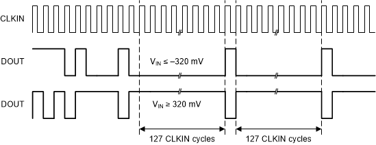
GUID-20201221-CA0I-ZCM1-CHGM-4429RMDKRPMK-low.gif Figure 7-5 Full-Scale Output of the AMC3306M25