SBAS997B February   2020  – October 2024 ADC09DJ1300-Q1 , ADC09QJ1300-Q1 , ADC09SJ1300-Q1

PRODUCTION DATA  

  1.   1
  2. Features
  3. Applications
  4. Description
  5. Pin Configuration and Functions
  6. Specifications
    1. 5.1  Absolute Maximum Ratings
    2. 5.2  ESD Ratings
    3. 5.3  Recommended Operating Conditions
    4. 5.4  Thermal Information
    5. 5.5  Electrical Characteristics: DC Specifications
    6. 5.6  Electrical Characteristics: Power Consumption
    7. 5.7  Electrical Characteristics: AC Specifications
    8. 5.8  Timing Requirements
    9. 5.9  Switching Characteristics
    10. 5.10 Typical Characteristics
  7. Detailed Description
    1. 6.1 Overview
    2. 6.2 Functional Block Diagram
    3. 6.3 Feature Description
      1. 6.3.1 Device Comparison
      2. 6.3.2 Analog Input
        1. 6.3.2.1 Analog Input Protection
        2. 6.3.2.2 Full-Scale Voltage (VFS) Adjustment
        3. 6.3.2.3 Analog Input Offset Adjust
        4. 6.3.2.4 ADC Core
          1. 6.3.2.4.1 ADC Core Calibration
          2. 6.3.2.4.2 ADC Theory of Operation
          3. 6.3.2.4.3 Analog Reference Voltage
          4. 6.3.2.4.4 ADC Over-range Detection
          5. 6.3.2.4.5 Code Error Rate (CER)
        5. 6.3.2.5 Temperature Monitoring Diode
        6. 6.3.2.6 Timestamp
        7. 6.3.2.7 Clocking
          1. 6.3.2.7.1 Converter PLL (C-PLL) for Sampling Clock Generation
          2. 6.3.2.7.2 LVDS Clock Outputs (PLLREFO±, TRIGOUT±)
          3. 6.3.2.7.3 Optional CMOS Clock Outputs (ORC, ORD)
          4. 6.3.2.7.4 SYSREF for JESD204C Subclass-1 Deterministic Latency
            1. 6.3.2.7.4.1 SYSREF Capture for Multi-Device Synchronization and Deterministic Latency
            2. 6.3.2.7.4.2 SYSREF Position Detector and Sampling Position Selection (SYSREF Windowing)
        8. 6.3.2.8 JESD204C Interface
          1. 6.3.2.8.1  Transport Layer
          2. 6.3.2.8.2  Scrambler
          3. 6.3.2.8.3  Link Layer
          4. 6.3.2.8.4  8B/10B Link Layer
            1. 6.3.2.8.4.1 Data Encoding (8B/10B)
            2. 6.3.2.8.4.2 Multiframes and the Local Multiframe Clock (LMFC)
            3. 6.3.2.8.4.3 Code Group Synchronization (CGS)
            4. 6.3.2.8.4.4 Initial Lane Alignment Sequence (ILAS)
            5. 6.3.2.8.4.5 Frame and Multiframe Monitoring
          5. 6.3.2.8.5  64B/66B Link Layer
            1. 6.3.2.8.5.1 64B/66B Encoding
            2. 6.3.2.8.5.2 Multiblocks, Extended Multiblocks and the Local Extended Multiblock Clock (LEMC)
              1. 6.3.2.8.5.2.1 Block, Multiblock and Extended Multiblock Alignment using Sync Header
                1. 6.3.2.8.5.2.1.1 Cyclic Redundancy Check (CRC) Mode
                2. 6.3.2.8.5.2.1.2 Forward Error Correction (FEC) Mode
            3. 6.3.2.8.5.3 Initial Lane Alignment
            4. 6.3.2.8.5.4 Block, Multiblock and Extended Multiblock Alignment Monitoring
          6. 6.3.2.8.6  Physical Layer
            1. 6.3.2.8.6.1 SerDes Pre-Emphasis
          7. 6.3.2.8.7  JESD204C Enable
          8. 6.3.2.8.8  Multi-Device Synchronization and Deterministic Latency
          9. 6.3.2.8.9  Operation in Subclass 0 Systems
          10. 6.3.2.8.10 Alarm Monitoring
            1. 6.3.2.8.10.1 Clock Upset Detection
            2. 6.3.2.8.10.2 FIFO Upset Detection
    4. 6.4 Device Functional Modes
      1. 6.4.1 Low Power Mode and High Performance Mode
      2. 6.4.2 JESD204C Modes
        1. 6.4.2.1 JESD204C Transport Layer Data Formats
        2. 6.4.2.2 64B/66B Sync Header Stream Configuration
        3. 6.4.2.3 Redundant Data Mode (Alternate Lanes)
      3. 6.4.3 Power-Down Modes
      4. 6.4.4 Test Modes
        1. 6.4.4.1  Serializer Test-Mode Details
        2. 6.4.4.2  PRBS Test Modes
        3. 6.4.4.3  Clock Pattern Mode
        4. 6.4.4.4  Ramp Test Mode
        5. 6.4.4.5  Short and Long Transport Test Mode
          1. 6.4.4.5.1 Short Transport Test Pattern
        6. 6.4.4.6  D21.5 Test Mode
        7. 6.4.4.7  K28.5 Test Mode
        8. 6.4.4.8  Repeated ILA Test Mode
        9. 6.4.4.9  Modified RPAT Test Mode
        10. 6.4.4.10 Calibration Modes and Trimming
          1. 6.4.4.10.1 Foreground Calibration Mode
          2. 6.4.4.10.2 Background Calibration Mode
          3. 6.4.4.10.3 Low-Power Background Calibration (LPBG) Mode
        11. 6.4.4.11 Offset Calibration
        12. 6.4.4.12 Trimming
    5. 6.5 Programming
      1. 6.5.1 Using the Serial Interface
      2. 6.5.2 SCS
      3. 6.5.3 SCLK
      4. 6.5.4 SDI
      5. 6.5.5 SDO
      6. 6.5.6 Streaming Mode
    6. 6.6 SPI_Register_Map Registers
  8. Application and Implementation
    1. 7.1 Application Information
    2. 7.2 Typical Applications
      1. 7.2.1 Light Detection and Ranging (LiDAR) Digitizer
        1. 7.2.1.1 Design Requirements
        2. 7.2.1.2 Detailed Design Procedure
          1. 7.2.1.2.1 Analog Front-End Requirements
          2. 7.2.1.2.2 Calculating Clock and SerDes Frequencies
        3. 7.2.1.3 Application Curves
        4. 7.2.1.4 Quad Channel Hand-Held 1.25-GSPS 625-MSPS Oscilloscope
      2. 7.2.2 Initialization Set Up
    3. 7.3 Power Supply Recommendations
      1. 7.3.1 Power Sequencing
    4. 7.4 Layout
      1. 7.4.1 Layout Guidelines
      2. 7.4.2 Layout Example
  9. Device and Documentation Support
    1. 8.1 Device Support
    2. 8.2 Documentation Support
    3. 8.3 Receiving Notification of Documentation Updates
    4. 8.4 Support Resources
    5. 8.5 Trademarks
    6. 8.6 Electrostatic Discharge Caution
    7. 8.7 Glossary
  10. Revision History
  11. 10Mechanical, Packaging, and Orderable Information

Application Curves

An example pulse measurement using the device is shown in Figure 7-2. The setup follows the example LiDAR system requirements with a 5-ns pulse captured at 1 GSPS . The applied pulse has a rise and fall time of approximately 1 ns. A sub-sampling technique is used to interpolate data points to form an equivalent 32 GSPS capture of the pulse for more accurate details and multiple capture averaging is used to suppress noise. A negative DC bias is applied to the ADC to enable use of the full dynamic range of the ADC for unipolar pulses. The pulse is spanning almost the full range of ADC codes. The extracted pulse parameters are given in Table 7-3. The analog front-end is not included in this measurement.
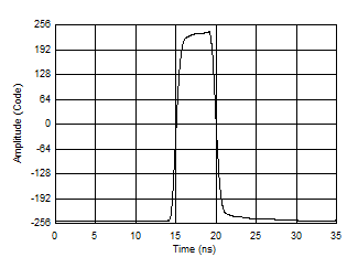
ADC09QJ1300-Q1 ADC09DJ1300-Q1 ADC09SJ1300-Q1 Measured Pulse using Sub-Sampling Technique for Equivalent 32 GSPS
                        MeasurementFigure 7-2 Measured Pulse using Sub-Sampling Technique for Equivalent 32 GSPS Measurement
Table 7-3 Extracted Pulse Parameters for Example LiDAR System
Measured ParameterMeasured ValueUnits
Rise Time (10-90%)1.18ns
Fall Time (90-10%)1.19ns
Pulse Width (50%)4.99ns
Equivalent Bandwidth(1)295.3MHz
Peak Amplitude (Codes)488LSB
Peak Amplitude (Voltage)750.6mV
DC Offset (Codes)-249LSB
DC Offset (Voltage)-383.7mV
The equivalent bandwidth is calculated from the extracted rise time measurement. The bandwidth is limited by a 1-ns transition time converter used at the output of the pulse generator.