SBASA52A July   2021  – October 2024 ADC12DJ800-Q1 , ADC12QJ800-Q1 , ADC12SJ800-Q1

PRODUCTION DATA  

  1.   1
  2. Features
  3. Applications
  4. Description
  5. Pin Configuration and Functions
  6. Specifications
    1. 5.1  Absolute Maximum Ratings
    2. 5.2  ESD Ratings
    3. 5.3  Recommended Operating Conditions
    4. 5.4  Thermal Information
    5. 5.5  Electrical Characteristics: DC Specifications
    6. 5.6  Electrical Characteristics: Power Consumption
    7. 5.7  Electrical Characteristics: AC Specifications
    8. 5.8  Timing Requirements
    9. 5.9  Switching Characteristics
    10. 5.10 Typical Characteristics
  7. Detailed Description
    1. 6.1 Overview
    2. 6.2 Functional Block Diagram
    3. 6.3 Feature Description
      1. 6.3.1 Device Comparison
      2. 6.3.2 Analog Input
        1. 6.3.2.1 Analog Input Protection
        2. 6.3.2.2 Full-Scale Voltage (VFS) Adjustment
        3. 6.3.2.3 Analog Input Offset Adjust
        4. 6.3.2.4 ADC Core
          1. 6.3.2.4.1 ADC Theory of Operation
          2. 6.3.2.4.2 ADC Core Calibration
          3. 6.3.2.4.3 Analog Reference Voltage
          4. 6.3.2.4.4 ADC Over-range Detection
          5. 6.3.2.4.5 Code Error Rate (CER)
      3. 6.3.3 Temperature Monitoring Diode
      4. 6.3.4 Timestamp
      5. 6.3.5 Clocking
        1. 6.3.5.1 Converter PLL (C-PLL) for Sampling Clock Generation
        2. 6.3.5.2 LVDS Clock Outputs (PLLREFO±, TRIGOUT±)
        3. 6.3.5.3 Optional CMOS Clock Outputs (ORC, ORD)
        4. 6.3.5.4 SYSREF for JESD204C Subclass-1 Deterministic Latency
          1. 6.3.5.4.1 SYSREF Capture for Multi-Device Synchronization and Deterministic Latency
          2. 6.3.5.4.2 SYSREF Position Detector and Sampling Position Selection (SYSREF Windowing)
      6. 6.3.6 JESD204C Interface
        1. 6.3.6.1  Transport Layer
        2. 6.3.6.2  Scrambler
        3. 6.3.6.3  Link Layer
        4. 6.3.6.4  8B/10B Link Layer
          1. 6.3.6.4.1 Data Encoding (8B/10B)
          2. 6.3.6.4.2 Multiframes and the Local Multiframe Clock (LMFC)
          3. 6.3.6.4.3 Code Group Synchronization (CGS)
          4. 6.3.6.4.4 Initial Lane Alignment Sequence (ILAS)
          5. 6.3.6.4.5 Frame and Multiframe Monitoring
        5. 6.3.6.5  64B/66B Link Layer
          1. 6.3.6.5.1 64B/66B Encoding
          2. 6.3.6.5.2 Multiblocks, Extended Multiblocks and the Local Extended Multiblock Clock (LEMC)
            1. 6.3.6.5.2.1 Block, Multiblock and Extended Multiblock Alignment using Sync Header
              1. 6.3.6.5.2.1.1 Cyclic Redundancy Check (CRC) Mode
              2. 6.3.6.5.2.1.2 Forward Error Correction (FEC) Mode
          3. 6.3.6.5.3 Initial Lane Alignment
          4. 6.3.6.5.4 Block, Multiblock and Extended Multiblock Alignment Monitoring
        6. 6.3.6.6  Physical Layer
          1. 6.3.6.6.1 SerDes Pre-Emphasis
        7. 6.3.6.7  JESD204C Enable
        8. 6.3.6.8  Multi-Device Synchronization and Deterministic Latency
        9. 6.3.6.9  Operation in Subclass 0 Systems
        10. 6.3.6.10 Alarm Monitoring
          1. 6.3.6.10.1 Clock Upset Detection
          2. 6.3.6.10.2 FIFO Upset Detection
    4. 6.4 Device Functional Modes
      1. 6.4.1 Low Power Mode and High Performance Mode
      2. 6.4.2 JESD204C Modes
        1. 6.4.2.1 JESD204C Transport Layer Data Formats
        2. 6.4.2.2 64B/66B Sync Header Stream Configuration
        3. 6.4.2.3 Redundant Data Mode (Alternate Lanes)
      3. 6.4.3 Power-Down Modes
      4. 6.4.4 Test Modes
        1. 6.4.4.1 Serializer Test-Mode Details
        2. 6.4.4.2 PRBS Test Modes
        3. 6.4.4.3 Clock Pattern Mode
        4. 6.4.4.4 Ramp Test Mode
        5. 6.4.4.5 Short and Long Transport Test Mode
          1. 6.4.4.5.1 Short Transport Test Pattern
        6. 6.4.4.6 D21.5 Test Mode
        7. 6.4.4.7 K28.5 Test Mode
        8. 6.4.4.8 Repeated ILA Test Mode
        9. 6.4.4.9 Modified RPAT Test Mode
      5. 6.4.5 Calibration Modes and Trimming
        1. 6.4.5.1 Foreground Calibration Mode
        2. 6.4.5.2 Background Calibration Mode
        3. 6.4.5.3 Low-Power Background Calibration (LPBG) Mode
      6. 6.4.6 Offset Calibration
      7. 6.4.7 Trimming
    5. 6.5 Programming
      1. 6.5.1 Using the Serial Interface
      2. 6.5.2 SCS
      3. 6.5.3 SCLK
      4. 6.5.4 SDI
      5. 6.5.5 SDO
      6. 6.5.6 Streaming Mode
      7. 6.5.7 SPI_Register_Map Registers
  8. Application and Implementation
    1. 7.1 Application Information
    2. 7.2 Typical Applications
      1. 7.2.1 Light Detection and Ranging (LiDAR) Digitizer
        1. 7.2.1.1 Design Requirements
        2. 7.2.1.2 Detailed Design Procedure
          1. 7.2.1.2.1 Analog Front-End Requirements
          2. 7.2.1.2.2 Calculating Clock and SerDes Frequencies
        3. 7.2.1.3 Application Curves
    3. 7.3 Initialization Set Up
    4. 7.4 Power Supply Recommendations
      1. 7.4.1 Power Sequencing
    5. 7.5 Layout
      1. 7.5.1 Layout Guidelines
      2. 7.5.2 Layout Example
  9. Device and Documentation Support
    1. 8.1 Device Support
    2. 8.2 Receiving Notification of Documentation Updates
    3. 8.3 Support Resources
    4. 8.4 Trademarks
    5. 8.5 Electrostatic Discharge Caution
    6. 8.6 Glossary
  10. Revision History
  11. 10Mechanical, Packaging, and Orderable Information

Description

ADC12xJ800-Q1 is a family of quad, dual and single channel, 12-bit, 800MSPS analog-to-digital converters (ADC). Low power consumption, high sampling rate and 12-bit resolution makes the ADC12xJ800-Q1 suited for light detection and ranging (LiDAR) systems. The ADC12xJ800-Q1 is qualified for automotive applications.

Full-power input bandwidth (-3dB) of 6GHz provides flat frequency response for frequency modulated continuous wave (FMCW) LiDAR systems and provides a narrow impulse response for pulse-based systems. The full-power input bandwidth also enables direct RF sampling of L-band and S-band.

A number of clocking features are included to relax system hardware requirements, such as an internal phase-locked loop (PLL) with integrated voltage-controlled oscillator (VCO) to generate the sampling clock. Four clock outputs are provided to clock the logic and SerDes of the FPGA or ASIC. A timestamp input and output is provided for pulsed systems.

JESD204C serialized interface decreases system size by reducing the amount of printed circuit board (PCB) routing. Interface modes support from 2 to 8 lanes (dual and quad channel devices) or 1 to 4 lanes (for the single channel device), with SerDes baud-rates up to 17.16Gbps, to allow the optimal configuration for each application.

Package Information
PART NUMBERPACKAGE(1)PACKAGE SIZE(2)
ADC12QJ800-Q1
ADC12DJ800-Q1
ADC12SJ800-Q1
FCBGA (144) 10mm × 10mm
For more information, see Section 10.
The package size (length × width) is a nominal value and includes pins, where applicable.
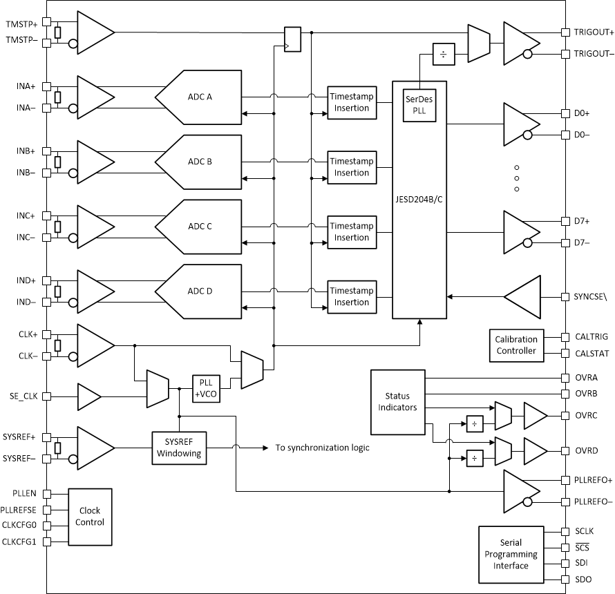
ADC12QJ800-Q1 ADC12DJ800-Q1 ADC12SJ800-Q1 Quad Channel Block Diagram Quad Channel Block Diagram