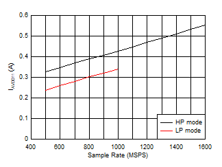
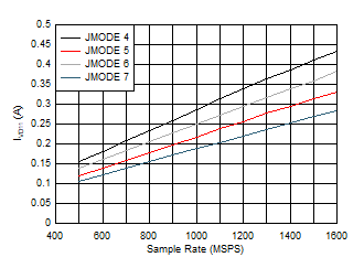
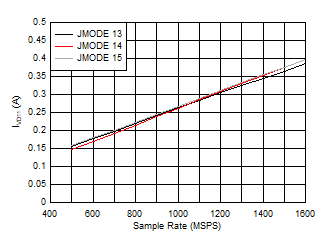
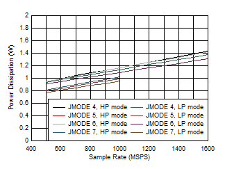
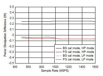
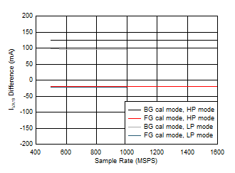
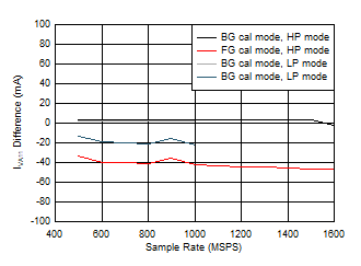
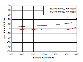
Typical values at 25°C, AIN
= -1 dBFS, FIN = 347 MHz, FS = 1600 MSPS, High power mode, FG
calibration, JMODE 0, C-PLL off, C-PLLREF = 50 MHz and VA11Q and VCLK11
noise suppression on when C-PLL on, Quad Channel operation, nominal supply voltages,
unless otherwise noted. SNR results exclude DC and HD2 to HD9; SINAD, ENOB, and SFDR
results exclude DC.
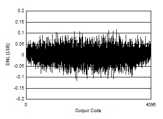
 Figure 5-1 DNL
vs Code
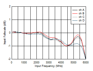
 Figure 5-3 Input
Fullscale vs Frequency
| High
power mode, C-PLL on |
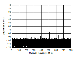
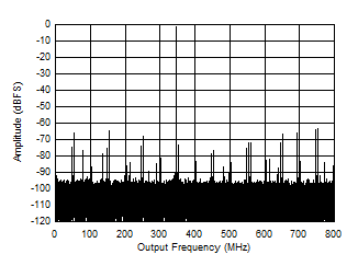
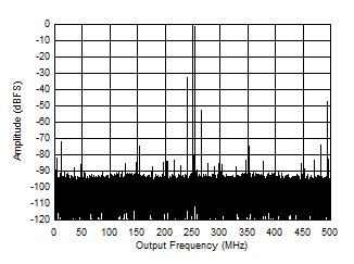
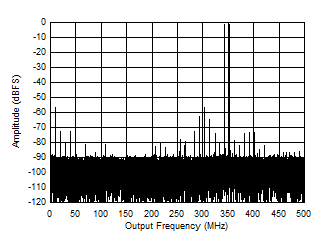
 Figure 5-7 Single Tone FFT at 847 MHz and -1 dBFS
| High
power mode, C-PLL on, Noise suppression off |
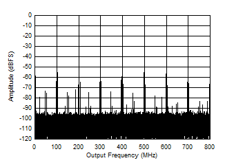
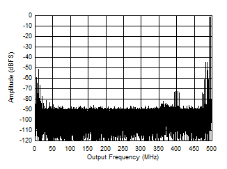
 Figure 5-11 Single Tone FFT at 3797 MHz and -1 dBFS
| C-PLL on, Low power mode, FS = 1000
MSPS |

| Low
power mode, FS = 1000 MSPS |
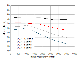
 Figure 5-17 SFDR
vs Input Frequency
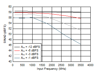
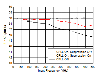
 Figure 5-19 SINAD
vs Input Frequency
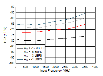
 Figure 5-21 HD2
vs Input Frequency
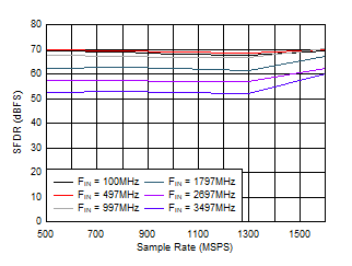
 Figure 5-23 SFDR
vs Sample Rate
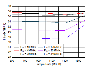
 Figure 5-25 SINAD
vs Sample Rate
 Figure 5-27 SFDR
vs Sample Rate
 Figure 5-29 SFDR
vs Sample Rate
 Figure 5-31 ENOB
vs Sample Rate
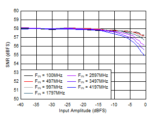
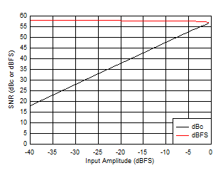
 Figure 5-33 SNR
vs AIN
| FIN = 100MHz, Low power mode |
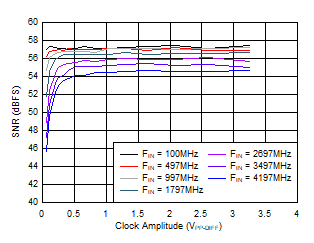
 Figure 5-37 SNR
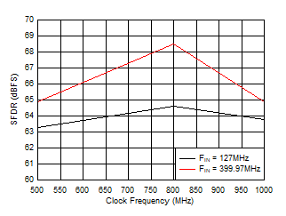
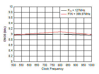
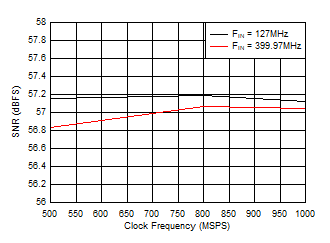
vs ACLK
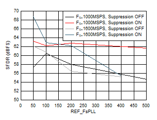
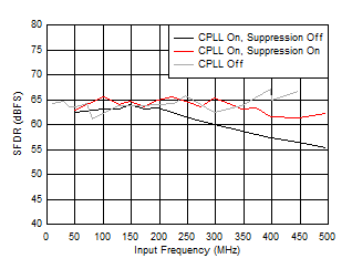
 Figure 5-39 SFDR
vs FREF and Suppression
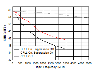
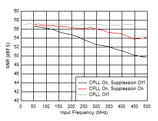
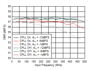
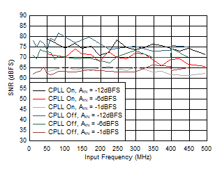
 Figure 5-41 SNR
vs FIN and C-PLL modes
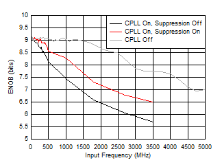
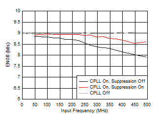
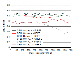
 Figure 5-43 ENOB
vs FIN and C-PLL modes
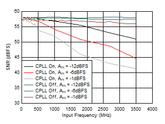
 Figure 5-45 SNR
vs FIN and C-PLL modes
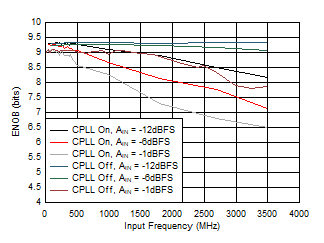
 Figure 5-47 ENOB
vs FIN and C-PLL modes
 Figure 5-49 SNR
vs AIN and C-PLL
 Figure 5-51 ENOB
vs AIN and C-PLL
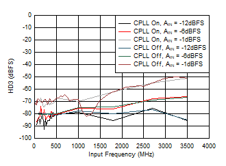
 Figure 5-53 HD3
vs AIN and C-PLL
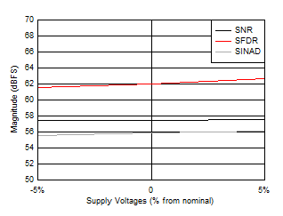
 Figure 5-55 SNR
vs AIN and C-PLL
 Figure 5-57 ENOB
vs AIN and C-PLL
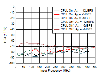
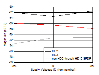
 Figure 5-59 HD3
vs AIN and C-PLL
| All
supplies changed together, high power mode |

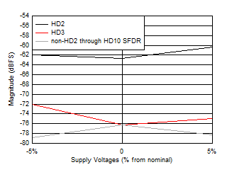
| All
supplies changed together, low power mode, FS
= 1000MSPS |
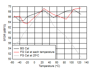
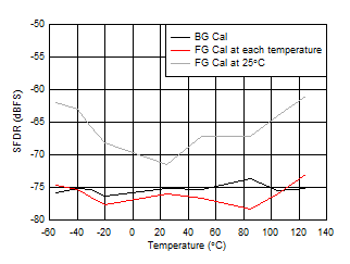
 Figure 5-65 SFDR
vs Temperature
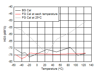
 Figure 5-67 HD3
vs Temperature
 Figure 5-69 Two
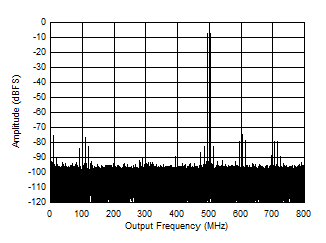
Tone FFT at 498MHz
 Figure 5-71 Two
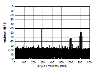
Tone FFT at 3498MHz
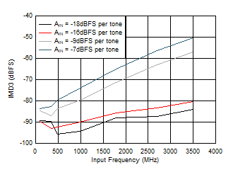
| 10
MHz tone spacing, -7 dBFS per tone, Low power mode,
1000MSPS |
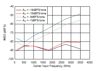
 Figure 5-75 IMD3
vs FIN
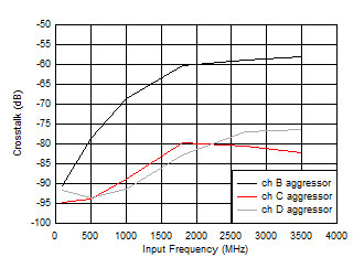
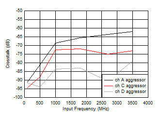
 Figure 5-77 Crosstalk to Channel A vs FIN
| Low
power background calibration mode |

| Low
power background calibration mode |

| Low
power background calibration mode, independent of
JMODE |

| Low
power background calibration mode, independent of power
mode |

| Low
power background calibration mode, independent of power
mode |

| Low
power background calibration mode |

| Low
power background calibration mode |

| Low
power background calibration mode, independent of
JMODE |

| Low
power background calibration mode, independent of power
mode |

| Low
power background calibration mode, independent of power
mode |

| Low
power background calibration mode |

| Low
power background calibration mode |

| Low
power background calibration mode, independent of
JMODE |

| Low
power background calibration mode |

| Low
power background calibration mode |

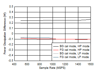
| Difference to lower power background calibration, JMODE
independent |

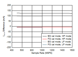
| Difference to lower power background calibration, JMODE
independent |

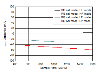
| Difference to lower power background calibration, JMODE
independent |

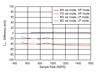
| Difference to lower power background calibration, JMODE
independent |

| Difference to lower power background calibration, JMODE
independent |

| Difference to lower power background calibration, JMODE
independent |
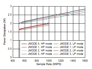
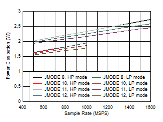
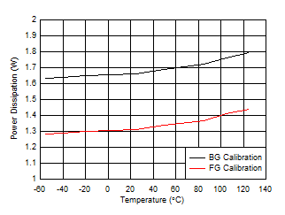
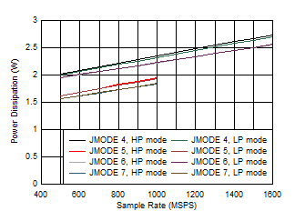
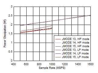
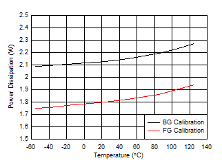
 Figure 5-121 Quad
Channel, Power Dissipation vs Temperature
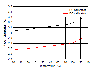
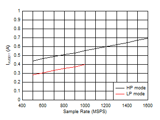
 Figure 5-123 Single Channel, Power Dissipation vs Temperature
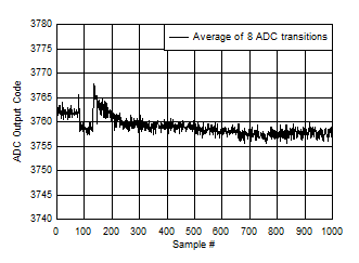
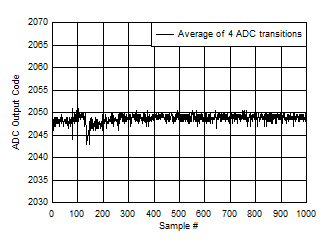
| BG
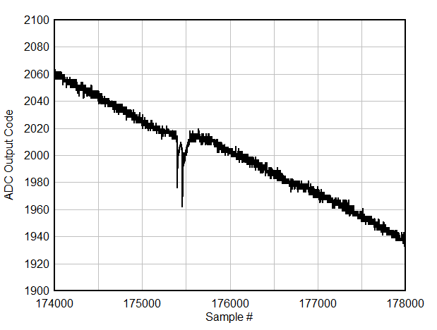
Calibration, input voltage offset ~ 90% of fullscale,
ADC_SRC_DLY=31, MUX_DLY=30 |

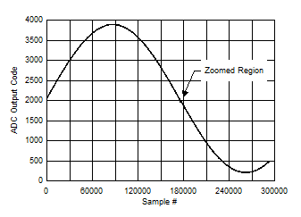
| BG
Calibration, ADC_SRC_DLY=31, MUX_DLY=30, unzoomed region
shown in previous plot |
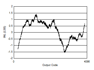
 Figure 5-2 INL
vs Code
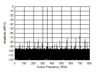
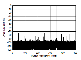
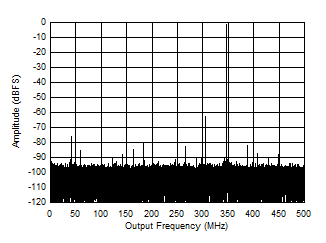
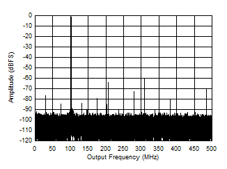
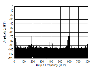
 Figure 5-4 Single Tone FFT at 347 MHz and -1 dBFS
| High
power mode, C-PLL on, Noise suppression off |

| High
power mode, C-PLL on |
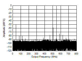
 Figure 5-10 Single Tone FFT at 1797 MHz and -1 dBFS
| Low
power mode, FS = 1000 MSPS |

| Low
power mode, FS = 1000 MSPS |

| Low
power mode, FS = 1000 MSPS |
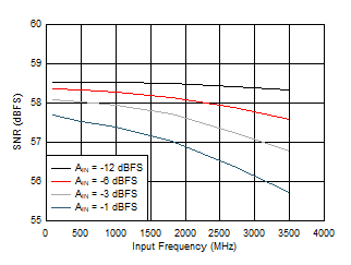
 Figure 5-18 SNR
vs Input Frequency
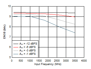
 Figure 5-20 ENOB
vs Input Frequency
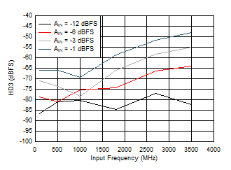
 Figure 5-22 HD3
vs Input Frequency
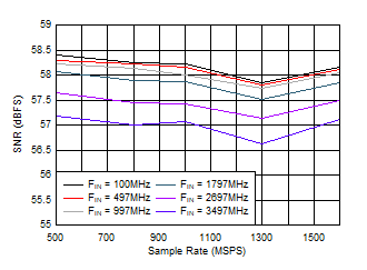
 Figure 5-24 SNR
vs Sample Rate
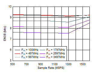
 Figure 5-26 ENOB
vs Sample Rate
 Figure 5-28 SNR
vs Sample Rate
 Figure 5-30 SINAD
vs Sample Rate
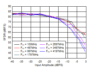
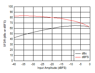
 Figure 5-32 SFDR
vs AIN
| FIN = 100MHz, Low power mode |
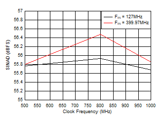
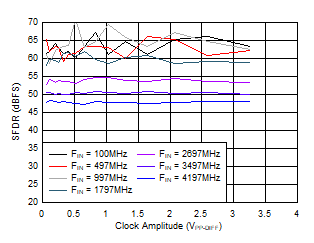
 Figure 5-36 SFDR
vs ACLK
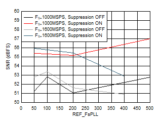
 Figure 5-38 SNR
vs FREF and Suppression
 Figure 5-40 SFDR
vs FIN and C-PLL modes
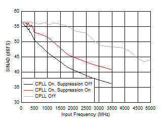
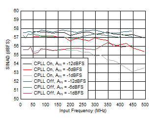
 Figure 5-42 SINAD
vs FIN and C-PLL modes
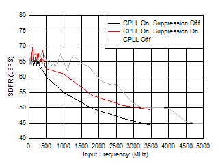
 Figure 5-44 SFDR
vs FIN and C-PLL modes
 Figure 5-46 SINAD
vs FIN and C-PLL modes
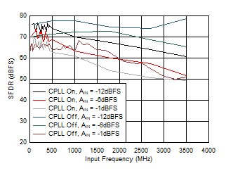
 Figure 5-48 SFDR
vs AIN and C-PLL
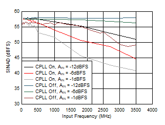
 Figure 5-50 SINAD
vs AIN and C-PLL
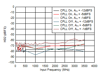
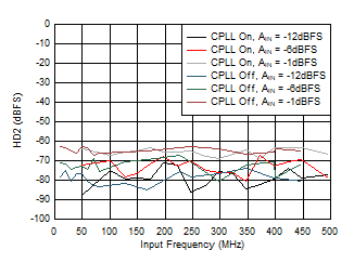
 Figure 5-52 HD2
vs AIN and C-PLL
 Figure 5-54 SFDR
vs AIN and C-PLL
 Figure 5-56 SINAD
vs AIN and C-PLL
 Figure 5-58 HD2
vs AIN and C-PLL
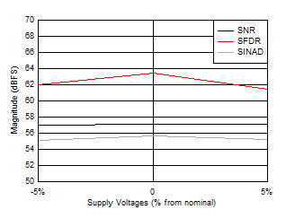
| All
supplies changed together, high power mode |

| All
supplies changed together, low power mode, FS
= 1000MSPS |
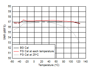
 Figure 5-64 SNR
vs Temperature
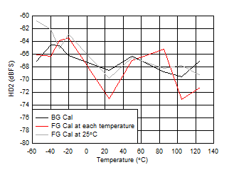
 Figure 5-66 HD2
vs Temperature
| Worst spur is non-HD2 though -HD10 SDFR |
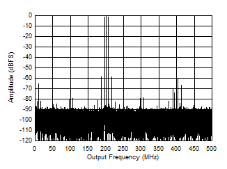
 Figure 5-70 Two
Tone FFT at 1798MHz
| 10
MHz tone spacing, -7 dBFS per tone, Low power mode,
1000MSPS |

| 10
MHz tone spacing, -7 dBFS per tone, Low power mode,
1000MSPS |

| 10MHz tone spacing, Low power mode, 1000MSPS |
 Figure 5-78 Crosstalk to Channel B vs FIN
| Low
power background calibration mode |

| Low
power background calibration mode |

| Low
power background calibration mode, independent of
JMODE |

| Low
power background calibration mode, independent of power
mode |

| Low
power background calibration mode, independent of power
mode |

| Low
power background calibration mode |

| Low
power background calibration mode |

| Low
power background calibration mode, independent of
JMODE |

| Low
power background calibration mode, independent of power
mode |

| Low
power background calibration mode, independent of power
mode |

| Low
power background calibration mode |

| Low
power background calibration mode |

| Low
power background calibration mode, independent of
JMODE |

| Low
power background calibration mode |

| Low
power background calibration mode |

| Difference to lower power background calibration, JMODE
independent |

| Difference to lower power background calibration, JMODE
independent |

| Difference to lower power background calibration, JMODE
independent |

| Difference to lower power background calibration, JMODE
independent |

| Difference to lower power background calibration, JMODE
independent |

| Difference to lower power background calibration, JMODE
independent |
 Figure 5-122 Dual
Channel, Power Dissipation vs Temperature
| BG
Calibration, midscale input voltage, ADC_SRC_DLY=31,
MUX_DLY=30 |

| BG
Calibration, ADC_SRC_DLY=31, MUX_DLY=30, zoomed region
shown in next plot |
