SBASB00 August 2024 AMC3306M25-Q1
PRODUCTION DATA
- 1
- 1 Features
- 2 Applications
- 3 Description
- 4 Pin Configuration and Functions
-
5 Specifications
- 5.1 Absolute Maximum Ratings
- 5.2 ESD Ratings
- 5.3 Recommended Operating Conditions
- 5.4 Thermal Information
- 5.5 Power Ratings
- 5.6 Insulation Specifications
- 5.7 Safety-Related Certifications
- 5.8 Safety Limiting Values
- 5.9 Electrical Characteristics
- 5.10 Switching Characteristics
- 5.11 Timing Diagrams
- 5.12 Insulation Characteristics Curves
- 5.13 Typical Characteristics
- 6 Detailed Description
- 7 Application and Implementation
- 8 Device and Documentation Support
- 9 Revision History
- 10Mechanical, Packaging, and Orderable Information
6.3.4 Digital Output
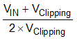
A differential input signal of 0V ideally produces a stream of ones and zeros that are high 50% of the time. A differential input of 250mV produces a stream of ones and zeros that are high 89.06% of the time. With 16 bits of resolution, that percentage corresponds to code 58368. A differential input of –250mV produces a stream of ones and zeros that are high 10.94% of the time and results in code 7168. These input voltages are also the specified linear range of the AMC3306M25-Q1. If the input voltage value exceeds this range, the output of the modulator shows nonlinear behavior as the quantization noise increases. The modulator output clips with constant stream of zeros with an input ≤ –320mV . In this case, the AMC3306M25-Q1 generates a single 1 every 128 clock cycles to indicate proper device function. The modulator output clips with constant stream of ones with an input ≥320mV. In this case, the AMC3306M25-Q1 generates a single 0 every 128 clock cycles to indicate proper device function. See the Output Behavior in Case of a Full-Scale Input section for more details. Figure 6-4 shows the input voltage versus the output modulator signal.
 Figure 6-4 AMC3306M25-Q1 Modulator Output vs Analog Input
Calculate the density of ones in the output bitstream with Equation 1 for any input voltage value except a full-scale input signal. See the Output Behavior in Case of a Full-Scale Input section.