SBASB12 May   2024 PCM1809

PRODUCTION DATA  

  1.   1
  2. Features
  3. Applications
  4. Description
  5. Pin Configuration and Functions
  6. Specifications
    1. 5.1 Absolute Maximum Ratings
    2. 5.2 ESD Ratings
    3. 5.3 Recommended Operating Conditions
    4. 5.4 Thermal Information
    5. 5.5 Electrical Characteristics
    6. 5.6 Timing Requirements: TDM, I2S or LJ Interface
    7. 5.7 Switching Characteristics: TDM, I2S or LJ Interface
    8. 5.8 Typical Characteristics
  7. Detailed Description
    1. 6.1 Overview
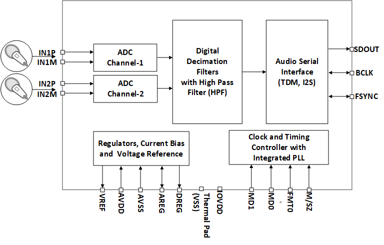
    2. 6.2 Functional Block Diagram
    3. 6.3 Feature Description
      1. 6.3.1 Hardware Control
      2. 6.3.2 Audio Serial Interfaces
        1. 6.3.2.1 Time Division Multiplexed Audio (TDM) Interface
        2. 6.3.2.2 Inter IC Sound (I2S) Interface
      3. 6.3.3 Phase-Locked Loop (PLL) and Clock Generation
      4. 6.3.4 Input Channel Configurations
      5. 6.3.5 Reference Voltage
      6. 6.3.6 Signal-Chain Processing
        1. 6.3.6.1 Digital High-Pass Filter
        2. 6.3.6.2 Configurable Digital Decimation Filters
          1. 6.3.6.2.1 Linear Phase Filters
            1. 6.3.6.2.1.1 Sampling Rate: 8 kHz or 7.35 kHz
            2. 6.3.6.2.1.2 Sampling Rate: 16 kHz or 14.7 kHz
            3. 6.3.6.2.1.3 Sampling Rate: 24 kHz or 22.05 kHz
            4. 6.3.6.2.1.4 Sampling Rate: 32 kHz or 29.4 kHz
            5. 6.3.6.2.1.5 Sampling Rate: 48 kHz or 44.1 kHz
            6. 6.3.6.2.1.6 Sampling Rate: 96 kHz or 88.2 kHz
            7. 6.3.6.2.1.7 Sampling Rate: 192 kHz or 176.4 kHz
          2. 6.3.6.2.2 Low-Latency Filters
            1. 6.3.6.2.2.1 Sampling Rate: 16 kHz or 14.7 kHz
            2. 6.3.6.2.2.2 Sampling Rate: 24 kHz or 22.05 kHz
            3. 6.3.6.2.2.3 Sampling Rate: 32 kHz or 29.4 kHz
            4. 6.3.6.2.2.4 Sampling Rate: 48 kHz or 44.1 kHz
            5. 6.3.6.2.2.5 Sampling Rate: 96 kHz or 88.2 kHz
    4. 6.4 Device Functional Modes
      1. 6.4.1 Active Mode
  8. Application and Implementation
    1. 7.1 Application Information
    2. 7.2 Typical Application
      1. 7.2.1 Design Requirements
      2. 7.2.2 Detailed Design Procedure
  9. Power Supply Recommendations
  10. Layout
    1. 9.1 Layout Guidelines
    2. 9.2 Layout Example
  11. 10Device and Documentation Support
    1. 10.1 Receiving Notification of Documentation Updates
    2. 10.2 Support Resources
    3. 10.3 Trademarks
    4. 10.4 Electrostatic Discharge Caution
    5. 10.5 Glossary
  12. 11Revision History
  13. 12Mechanical, Packaging, and Orderable Information

Functional Block Diagram

PCM1809