SBASB12 May 2024 PCM1809
PRODUCTION DATA
- 1
- 1 Features
- 2 Applications
- 3 Description
- 4 Pin Configuration and Functions
- 5 Specifications
-
6 Detailed Description
- 6.1 Overview
- 6.2 Functional Block Diagram
- 6.3
Feature Description
- 6.3.1 Hardware Control
- 6.3.2 Audio Serial Interfaces
- 6.3.3 Phase-Locked Loop (PLL) and Clock Generation
- 6.3.4 Input Channel Configurations
- 6.3.5 Reference Voltage
- 6.3.6
Signal-Chain Processing
- 6.3.6.1 Digital High-Pass Filter
- 6.3.6.2
Configurable Digital Decimation Filters
- 6.3.6.2.1
Linear Phase Filters
- 6.3.6.2.1.1 Sampling Rate: 8 kHz or 7.35 kHz
- 6.3.6.2.1.2 Sampling Rate: 16 kHz or 14.7 kHz
- 6.3.6.2.1.3 Sampling Rate: 24 kHz or 22.05 kHz
- 6.3.6.2.1.4 Sampling Rate: 32 kHz or 29.4 kHz
- 6.3.6.2.1.5 Sampling Rate: 48 kHz or 44.1 kHz
- 6.3.6.2.1.6 Sampling Rate: 96 kHz or 88.2 kHz
- 6.3.6.2.1.7 Sampling Rate: 192 kHz or 176.4 kHz
- 6.3.6.2.2 Low-Latency Filters
- 6.3.6.2.1
Linear Phase Filters
- 6.4 Device Functional Modes
- 7 Application and Implementation
- 8 Power Supply Recommendations
- 9 Layout
- 10Device and Documentation Support
- 11Revision History
- 12Mechanical, Packaging, and Orderable Information
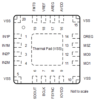
4 Pin Configuration and Functions
 Figure 4-1 RTE
Package,20-Pin
WQFN With Exposed Thermal Pad,Top View
Figure 4-1 RTE
Package,20-Pin
WQFN With Exposed Thermal Pad,Top ViewTable 4-1 Pin Functions
| PIN | TYPE | DESCRIPTION | |
|---|---|---|---|
| NO. | NAME | ||
| 1 | IN1P | Analog input | Analog input 1P pin. |
| 2 | IN1M | Analog input | Analog input 1M pin. |
| 3 | IN2P | Analog input | Analog input 2P pin. |
| 4 | IN2M | Analog input | Analog input 2M pin. |
| 5 | VSS | Analog Supply | Short this pin directly to the board ground plane. |
| 6 | SDOUT | Digital output | Audio serial data interface bus output. |
| 7 | BCLK | Digital I/O | Audio serial data interface bus bit clock. |
| 8 | FSYNC | Digital I/O | Audio serial data interface bus frame synchronization signal. |
| 9 | IOVDD | Digital supply | Digital I/O power supply (1.8 V or 3.3 V, nominal). |
| 10 | VSS | Analog supply | Short this pin directly to the board ground plane. |
| 11 | MD1 | Digital input | Device configuration mode select 1 pin. |
| 12 | MD0 | Digital input | Device configuration mode select 0 pin. |
| 13 | MSZ | Digital input | Audio interface bus controller or target select pin. |
| 14 | DREG | Digital supply | Digital regulator output voltage for digital core supply (1.5 V, nominal). |
| 15 | VSS | Analog supply | Short this pin directly to the board ground plane. |
| 16 | AVDD | Analog supply | Analog power (3.3 V, nominal). |
| 17 | AREG | Analog supply | Analog on-chip regulator output voltage for analog supply (1.8 V, nominal). |
| 18 | VREF | Analog | Analog reference voltage filter output. |
| 19 | FMT0 | Digital input | Audio interface format select pin referred to AVDD supply. |
| 20 | VSS | Analog supply | Short this pin directly to the board ground plane. |
| Thermal Pad (VSS) | Ground supply | Thermal pad shorted to internal device ground. Short thermal pad directly to board ground plane. | |