SBASB12 May 2024 PCM1809
PRODUCTION DATA
- 1
- 1 Features
- 2 Applications
- 3 Description
- 4 Pin Configuration and Functions
- 5 Specifications
-
6 Detailed Description
- 6.1 Overview
- 6.2 Functional Block Diagram
- 6.3
Feature Description
- 6.3.1 Hardware Control
- 6.3.2 Audio Serial Interfaces
- 6.3.3 Phase-Locked Loop (PLL) and Clock Generation
- 6.3.4 Input Channel Configurations
- 6.3.5 Reference Voltage
- 6.3.6
Signal-Chain Processing
- 6.3.6.1 Digital High-Pass Filter
- 6.3.6.2
Configurable Digital Decimation Filters
- 6.3.6.2.1
Linear Phase Filters
- 6.3.6.2.1.1 Sampling Rate: 8 kHz or 7.35 kHz
- 6.3.6.2.1.2 Sampling Rate: 16 kHz or 14.7 kHz
- 6.3.6.2.1.3 Sampling Rate: 24 kHz or 22.05 kHz
- 6.3.6.2.1.4 Sampling Rate: 32 kHz or 29.4 kHz
- 6.3.6.2.1.5 Sampling Rate: 48 kHz or 44.1 kHz
- 6.3.6.2.1.6 Sampling Rate: 96 kHz or 88.2 kHz
- 6.3.6.2.1.7 Sampling Rate: 192 kHz or 176.4 kHz
- 6.3.6.2.2 Low-Latency Filters
- 6.3.6.2.1
Linear Phase Filters
- 6.4 Device Functional Modes
- 7 Application and Implementation
- 8 Power Supply Recommendations
- 9 Layout
- 10Device and Documentation Support
- 11Revision History
- 12Mechanical, Packaging, and Orderable Information
3 Description
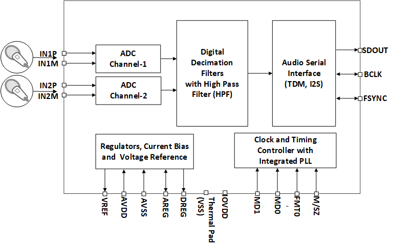
The PCM1809 is a low power audio analog-to-digital converter (ADC) that supports simultaneous sampling of up to two analog channels. The device supports single-ended and differential line and microphone inputs with a 2VRMS full-scale differential signal. The device integrates a phase-locked loop (PLL), a DC removal high-pass filter (HPF), and supports sample rates up to 192kHz. The device supports time-division multiplexing (TDM) or I2S audio formats, selectable with the hardware pin level. Additionally, the PCM1809 supports Controller and target mode selection for the audio bus interface operation. These integrated features, along with the ability to be powered from a single supply of 3.3V, make the device an excellent choice for cost-sensitive, space-constrained audio systems in microphone recording applications.
The PCM1809 is specified from –40°C to +105°C, and is offered in a 20-pin WQFN package.
| PART NUMBER | PACKAGE(1) | PACKAGE SIZE(2) |
|---|---|---|
| PCM1809 | WQFN (20) | 3.00mm × 3.00mm with 0.5mm pitch |
 Simplified
Block Diagram