SBASB20 September   2024 DDS39RF10 , DDS39RFS10

PRODUCTION DATA  

  1.   1
  2. Features
  3. Applications
  4. Description
  5. Device Comparison
  6. Pin Configuration and Functions
  7. Specifications
    1. 6.1  Absolute Maximum Ratings
    2. 6.2  ESD Ratings
    3. 6.3  Recommended Operating Conditions
    4. 6.4  Thermal Information
    5. 6.5  Electrical Characteristics - DC Specifications
    6. 6.6  Electrical Characteristics - AC Specifications
    7. 6.7  Electrical Characteristics - Power Consumption
    8. 6.8  Timing Requirements
    9. 6.9  Switching Characteristics
    10. 6.10 SPI and FRI Timing Diagrams
    11. 6.11 Typical Characteristics: Single Tone Spectra
    12. 6.12 Typical Characteristics: Dual Tone Spectra
    13. 6.13 Typical Characteristics: Power Dissipation and Supply Currents
  8. Detailed Description
    1. 7.1 Overview
    2. 7.2 Functional Block Diagrams
    3. 7.3 Feature Description
      1. 7.3.1 DAC Output Modes
        1. 7.3.1.1 NRZ Mode
        2. 7.3.1.2 RTZ Mode
        3. 7.3.1.3 RF Mode
        4. 7.3.1.4 DES Mode
      2. 7.3.2 DAC Core
        1. 7.3.2.1 DAC Output Structure
        2. 7.3.2.2 Full-Scale Current Adjustment
      3. 7.3.3 DEM and Dither
      4. 7.3.4 Offset Adjustment
      5. 7.3.5 Clocking Subsystem
        1. 7.3.5.1 SYSREF Frequency Requirements
        2. 7.3.5.2 SYSREF Position Detector and Sampling Position Selection (SYSREF Windowing)
      6. 7.3.6 Digital Signal Processing Blocks
        1. 7.3.6.1 Digital Upconverter (DUC)
          1. 7.3.6.1.1 Interpolation Filters
          2. 7.3.6.1.2 Numerically Controlled Oscillator (NCO)
            1. 7.3.6.1.2.1 Phase-Continuous NCO Update Mode
            2. 7.3.6.1.2.2 Phase-coherent NCO Update Mode
            3. 7.3.6.1.2.3 Phase-sync NCO Update Mode
            4. 7.3.6.1.2.4 NCO Synchronization
              1. 7.3.6.1.2.4.1 JESD204C LSB Synchonization
            5. 7.3.6.1.2.5 NCO Mode Programming
          3. 7.3.6.1.3 Mixer Scaling
        2. 7.3.6.2 Channel Bonder
        3. 7.3.6.3 DES Interpolator
      7. 7.3.7 JESD204C Interface
        1. 7.3.7.1  Deviation from JESD204C Standard
        2. 7.3.7.2  Transport Layer
        3. 7.3.7.3  Scrambler and Descrambler
        4. 7.3.7.4  Link Layer
        5. 7.3.7.5  Physical Layer
        6. 7.3.7.6  Serdes PLL Control
        7. 7.3.7.7  Serdes Crossbar
        8. 7.3.7.8  Multi-Device Synchronization and Deterministic Latency
          1. 7.3.7.8.1 Programming RBD
        9. 7.3.7.9  Operation in Subclass 0 Systems
        10. 7.3.7.10 Link Reset
      8. 7.3.8 Alarm Generation
    4. 7.4 Device Functional Modes
      1. 7.4.1 DUC and DDS Modes
      2. 7.4.2 JESD204C Interface Modes
        1. 7.4.2.1 JESD204C Interface Modes
        2. 7.4.2.2 JESD204C Format Diagrams
          1. 7.4.2.2.1 16-bit Formats
      3. 7.4.3 NCO Synchronization Latency
      4. 7.4.4 Data Path Latency
    5. 7.5 Programming
      1. 7.5.1 Using the Standard SPI Interface
        1. 7.5.1.1 SCS
        2. 7.5.1.2 SCLK
        3. 7.5.1.3 SDI
        4. 7.5.1.4 SDO
        5. 7.5.1.5 Serial Interface Protocol
        6. 7.5.1.6 Streaming Mode
      2. 7.5.2 Using the Fast Reconfiguration Interface
      3. 7.5.3 SPI Register Map
  9. Application and Implementation
    1. 8.1 Application Information
      1. 8.1.1 Startup Procedure for DUC/Bypass Mode
      2. 8.1.2 Startup Procedure for DDS Mode
      3. 8.1.3 Understanding Dual Edge Sampling Modes
      4. 8.1.4 Eye Scan Procedure
      5. 8.1.5 Pre/Post Cursor Analysis Procedure
      6. 8.1.6 Sleep and Disable Modes
    2. 8.2 Typical Application
      1. 8.2.1 S-Band Radar Transmitter
      2. 8.2.2 Design Requirements
      3. 8.2.3 Detailed Design Procedure
      4. 8.2.4 Detailed Clocking Subsystem Design Procedure
        1. 8.2.4.1 Example 1: SWAP-C Optimized
        2. 8.2.4.2 Example 2: Improved Phase Noise LMX2820 with External VCO
        3. 8.2.4.3 Example 3: Discrete Analog PLL for Best DAC Performance
        4. 8.2.4.4 10GHz Clock Generation
      5. 8.2.5 Application Curves
    3. 8.3 Power Supply Recommendations
      1. 8.3.1 Power Up and Down Sequence
    4. 8.4 Layout
      1. 8.4.1 Layout Guidelines and Example
  10. Device and Documentation Support
    1. 9.1 Receiving Notification of Documentation Updates
    2. 9.2 Support Resources
    3. 9.3 Trademarks
    4. 9.4 Electrostatic Discharge Caution
    5. 9.5 Glossary
  11. 10Revision History
  12. 11Mechanical, Packaging, and Orderable Information
Phase-coherent NCO Update Mode

The phase-coherent NCO update mode, the frequency word is updated and is multiplied by a counter to update the accumulator. This allows the phase for a particular frequency to be "coherent" with the previous usage of the frequency as if the NCO had never been tuned away from that frequency. Since the phase information is maintained by the counter, any frequency can be phase coherent. Phase Coherent NCO Mode operation is demonstrated in Figure 7-45 and selected by programming NCO_CONT = 0 and NCO_AR = 0. If alignment between multiple devices is required, then NCO_AR must be programmed to 1 during the initial NCO synchronization to align the master accumulator for all devices.
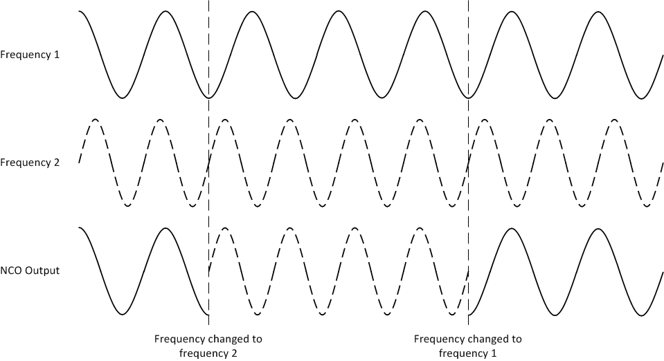
DDS39RF10 DDS39RFS10 Example Phase Coherent NCO Mode OperationFigure 7-45 Example Phase Coherent NCO Mode Operation