SBASB21 September 2024 DDS39RF12 , DDS39RFS12
PRODUCTION DATA
- 1
- 1 Features
- 2 Applications
- 3 Description
- 4 Device Comparison
- 5 Pin Configuration and Functions
-
6 Specifications
- 6.1 Absolute Maximum Ratings
- 6.2 ESD Ratings
- 6.3 Recommended Operating Conditions
- 6.4 Thermal Information
- 6.5 Electrical Characteristics - DC Specifications
- 6.6 Electrical Characteristics - AC Specifications
- 6.7 Electrical Characteristics - Power Consumption
- 6.8 Timing Requirements
- 6.9 Switching Characteristics
- 6.10 SPI and FRI Timing Diagrams
- 6.11 Typical Characteristics: Single Tone Spectra
- 6.12 Typical Characteristics: Dual Tone Spectra
- 6.13 Typical Characteristics: Power Dissipation and Supply Currents
-
7 Detailed Description
- 7.1 Overview
- 7.2 Functional Block Diagrams
- 7.3
Feature Description
- 7.3.1 DAC Output Modes
- 7.3.2 DAC Core
- 7.3.3 DEM and Dither
- 7.3.4 Offset Adjustment
- 7.3.5 Clocking Subsystem
- 7.3.6 Digital Signal Processing Blocks
- 7.3.7
JESD204C Interface
- 7.3.7.1 Deviation from JESD204C Standard
- 7.3.7.2 Transport Layer
- 7.3.7.3 Scrambler and Descrambler
- 7.3.7.4 Link Layer
- 7.3.7.5 Physical Layer
- 7.3.7.6 Serdes PLL Control
- 7.3.7.7 Serdes Crossbar
- 7.3.7.8 Multi-Device Synchronization and Deterministic Latency
- 7.3.7.9 Operation in Subclass 0 Systems
- 7.3.7.10 Link Reset
- 7.3.8 Alarm Generation
- 7.4 Device Functional Modes
- 7.5 Programming
- 8 Application and Implementation
- 9 Device and Documentation Support
- 10Revision History
- 11Mechanical, Packaging, and Orderable Information
7.3.7.8.1 Programming RBD
The range of values for RBD depends on the phase delta between the Rx and Tx LMFC/LEMC, as well as link latencies in the Tx, channel, and Rx. Therefore, do not provide a pre-determined RBD value that is appropriate for all systems. The LANE_ARR registers are provided to help the user measure lane arrival times and select an appropriate RBD value for the system. For deterministic latency, the RBD value can be selected during system prototyping and stored in system firmware. Calculating RBD each time the system is turned on can result in non-deterministic latency.
The arrival times are reported in units of quad-bytes and are measured with respect to a modulo-64 reference counter that increments for each quad-byte received (per lane). The reference counter is aligned (reset) by SYSREF.
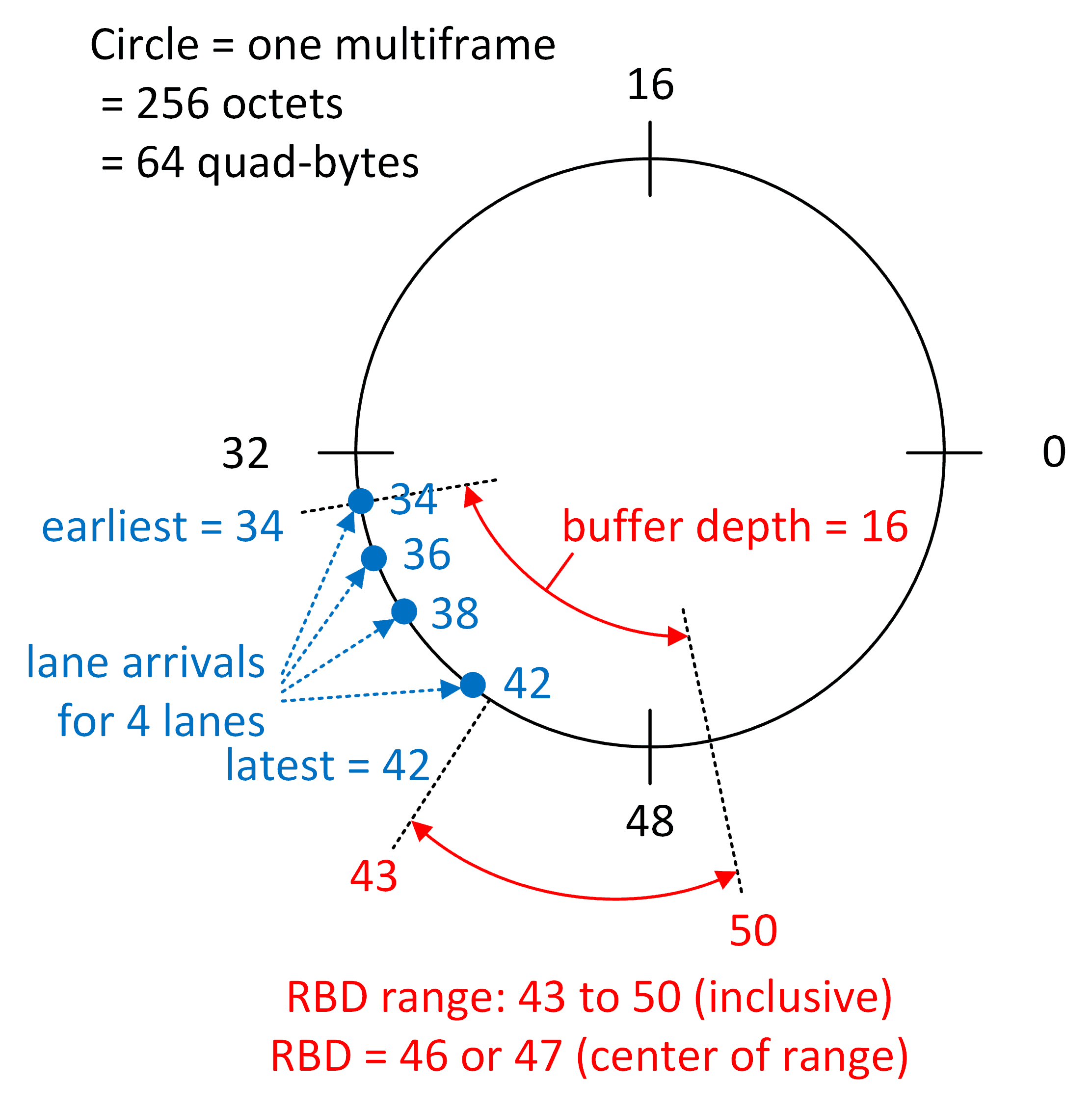
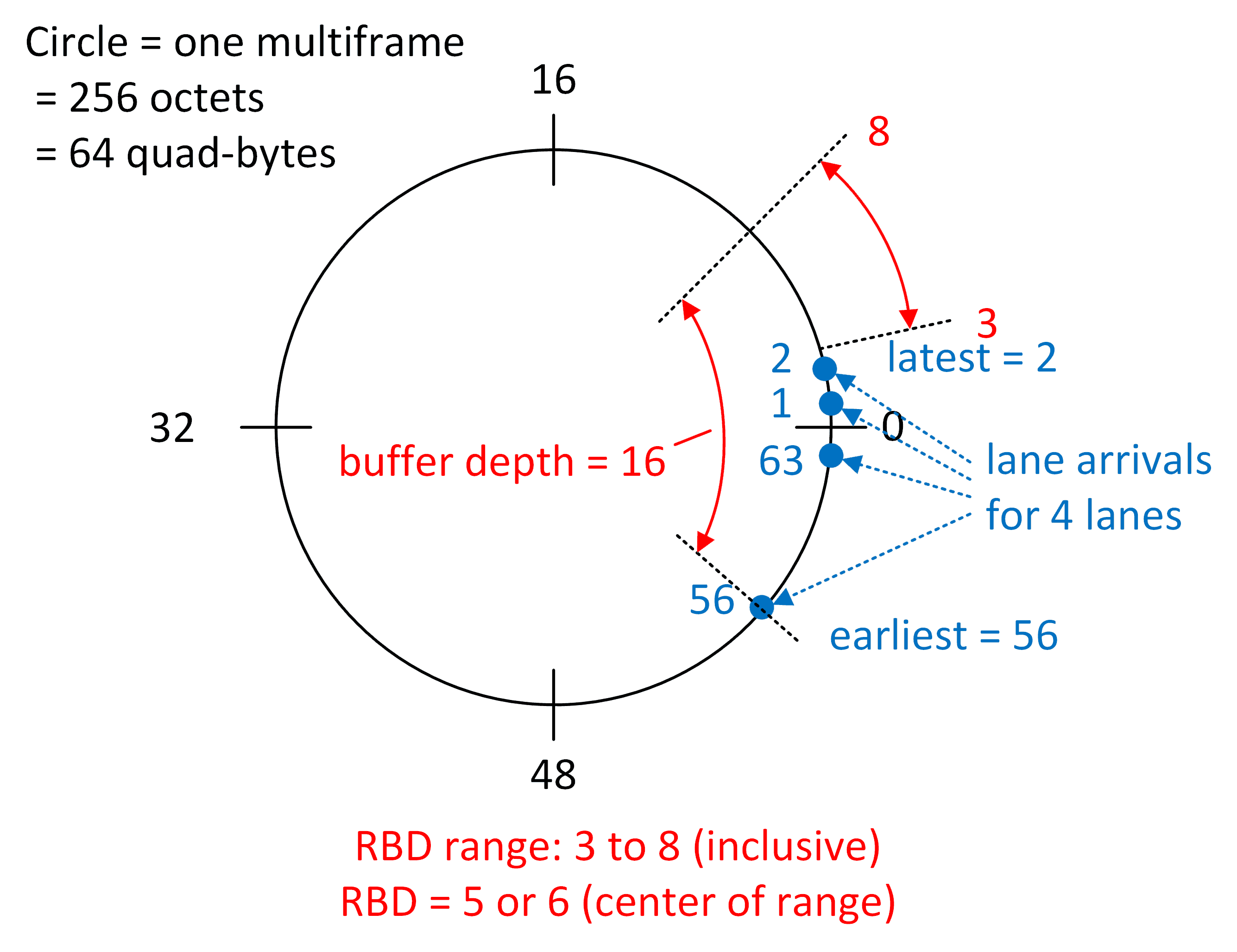
Since the lane arrival times are modulo-values, it is important to use arithmetic that accounts for the modulus (the latest arriving lane might actually have a smaller LANE_ARR value than the earliest arriving lane). Figure 7-55 and Figure 7-56 depict the RBD calculation graphically to emphasize this. The lane arrival times are mapped onto a circle with a circumference of 64 quad-bytes which corresponds to the modulo-64 counter used to measure lane arrival times.
The earliest usable RBD value is equal to the latest LANE_ARR value plus 1 (modulo 64). The latest usable RBD value is equal to the earliest LANE_ARR value plus the buffer depth (modulo 64) (the buffer depth is 16 quad-octets, except when K x F = 32, then the buffer depth is reduced to 8 quad-octets). Note that the latest, usable RBD value causes the earliest arriving lane to overwrite buffer data on the same clock cycle that the data is being read out (this is acceptable and does not cause overflow).
Choosing an RBD value in the middle of the usable range maximizes the skew tolerance; however, the user can choose a value closer to the latest arriving lane if lower latency is desired.
 Figure 7-55 RBD Example (lane arrivals do not straddle zero)
 Figure 7-56 RBD Example (lane arrivals straddle zero)