SBAU383A June 2021 – February 2022 BUF802
9 Layout Prints
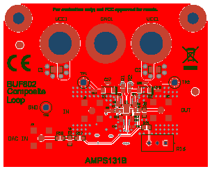
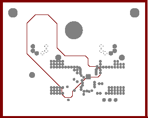
Figure 9-1 through Figure 9-8 show the PCB layers for the BUF802RGTEVM standalone circuit and composite circuit respectively.
 Figure 9-1 Standalone Configuration
Top Layers
 Figure 9-3 Standalone Configuration
Power Layer
 Figure 9-5 Composite Configuration
Top Layers
 Figure 9-7 Composite Configuration
Power Layer
 Figure 9-2 Standalone Configuration
Ground Layer
 Figure 9-4 Standalone Configuration
Bottom Layers
 Figure 9-6 Composite Configuration
Ground Layer
 Figure 9-8 Composite Configuration
Bottom Layers