SBAU413A october   2022  – may 2023


  1.   Abstract
  2.   Trademarks
  3. 1EVM Overview
    1. 1.1 ADS131B26Q1EVM-PDK Features
    2. 1.2 ADS131B26Q1EVM-PDK Quick-Start Guide
  4. 2Analog Interface
    1. 2.1 Terminal Blocks and Test Points
    2. 2.2 ADC1A and ADC1B
    3. 2.3 ADC2A and ADC2B
    4. 2.4 ADC3A and ADC3B
  5. 3Digital Interface
    1. 3.1 Connection to the PHI Controller
    2. 3.2 Digital Header
    3. 3.3 Clock Options
  6. 4Power Supplies
    1. 4.1 DC/DC Converter Circuit
    2. 4.2 ADC Power Supplies
    3. 4.3 Power Supply and Voltage Reference Decoupling
  7. 5ADS131B26Q1EVM-PDK Initial Setup
    1. 5.1 Default Jumper Settings
    2. 5.2 EVM Graphical User Interface (GUI) Software Installation
  8. 6ADS131B26Q1EVM-PDK Software Reference
    1. 6.1 Global Settings for ADC Control
    2. 6.2 Register Map Configuration
      1. 6.2.1 Register Map Basics
      2. 6.2.2 ADC1A, ADC3A and ADC1B, ADC3B Configuration
      3. 6.2.3 ADC2A and ADC2B Configuration
    3. 6.3 Analysis Tools
      1. 6.3.1 Time Domain Display
      2. 6.3.2 Spectral Analysis Tool
      3. 6.3.3 Histogram Analysis
      4. 6.3.4 Sequencer Analysis
  9. 7ADS131B26Q1EVM-PDK Bill of Materials, PCB Layout, and Schematics
    1. 7.1 Bill of Materials (BOM)
    2. 7.2 PCB Layout
    3. 7.3 Schematics
  10. 8Revision History

Schematics

Figure 7-7 and Figure 7-8 contain the schematics for the ADS131B26Q1EVM-PDK.

GUID-20230502-SS0I-BFTC-3BSS-R2CR9PTQZ9HH-low.svg Figure 7-7 Analog Inputs, ADC Power, and Interface Connections
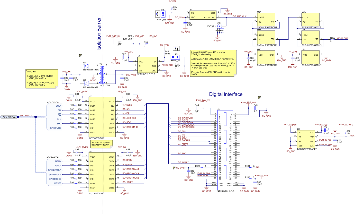
GUID-20220920-SS0I-PWBQ-Q9XJ-B4BNFBZSVS4P-low.gif Figure 7-8 Digital Isolators, DC/DC Power Supply, External Clock, and PHI Controller
GUID-20230502-SS0I-RFRQ-KWBP-BVQP4LGD4FD8-low.svg Figure 7-9 Hardware, Logos, Miscellaneous