SBAU467 October 2024 ADC32RF55
- 1
- Description
- Features
- Applications
- 5
- 1Evaluation Module Overview
- 2Hardware
- 3Quick Start Guide
- 4Hardware Design Files
- 5Additional Information
- 6Related Documentation
4.2 PCB Layouts
 Figure 4-3 Channel A RF Layout
 Figure 4-4 Channel B RF Layout
Exemplified in this EVM are common best practices when laying out an RF PCB. Included in this design are stitching vias located to connect the top ground plane to the ground plane directly adjacent. This allows the transmission line created by the RF trace to present a constant impedance as possible.
In general, if possible, avoid passing RF traces through vias to different layers. However, in some cases, like this one, this is necessary as the pinout of the TRF1305 and the ADC CHB are reversed requiring routing through the bottom layer and the middle layer of the PCB, as seen in Figure 4-4. Additional losses are avoided here by utilizing stitching vias and controlled lengths.
Additionally, seen on CHA top layer is the onboard resistive power divider, which is uninstalled as default. Utilization of the onboard resistive divider allows the user to evaluate the pros and cons of incorporating such a divider into the end equipments.
 Figure 4-5 RF Ground Layer
The RF ground layer has been notched underneath each of the component pads to present as little excess capacitance to the transmission line above as possible. Other than this, the ground layer has been laid out to be as contiguous as possible to limit excess inductance.
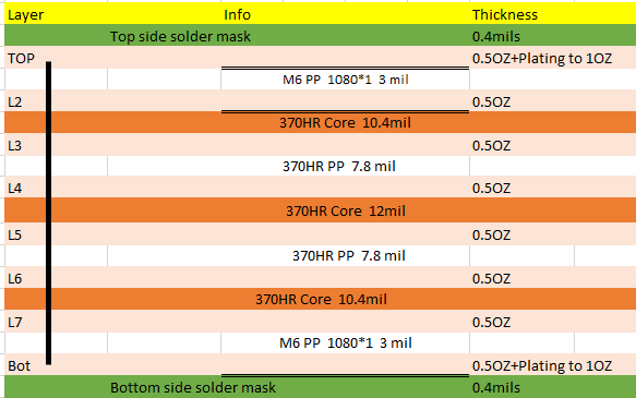
 Figure 4-6 Board Stackup
The dielectric in this case was chosen as Panasonic Megtron6. This dielectric was chosen for the controlled dielectric constant. The effects of this are constant and controlled impedance of the surrounding RF traces.