SBOA213B February 2018 – October 2024 OPA1612 , OPA172
Design Goals
| Input | Output | Supply | ||||
|---|---|---|---|---|---|---|
| ViMin | ViMax | VoMin | VoMax | Vcc | Vee | Vref |
| 100mVpp | 50Vpp | 1mVpp | 500mVpp | 15V | –15V | 0V |
Design Description
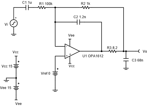
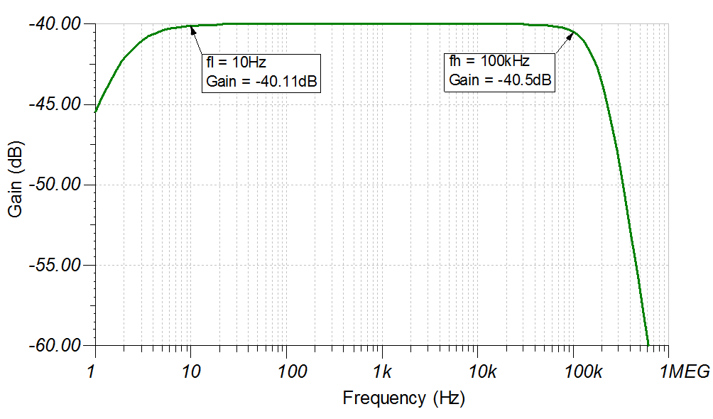
This tunable band-pass attenuator reduces signal level by –40dB over the frequency range from 10Hz to 100kHz. It also allows for independent control of the DC output level. For this design, the pole frequencies were selected outside the pass band to minimize attenuation within the specified bandwidth range.

Design Notes
- If a DC voltage is applied to Vref be sure to check common mode limitations.
- Keep R3 as small as possible to avoid loading issues while maintaining stability.
- Keep the frequency of the second pole in the low-pass filter (fp3) at least twice the frequency of the first low-pass filter pole (fp2).
Design Steps
- Set the pass-band gain.
- Set high-pass filter pole frequency
(fp1) below fl.
- Set low-pass filter pole frequency
(fp2 and fp3) above fh.
- Calculate C1 to set the
location of fp1.
- Select components to set
fp2 and fp3.
Design Simulations
DC Simulation Results
The amplifier passes DC voltages applied to the noninverting pin up to the common mode limitations of the op amp (±13V in this design)
AC Simulation Results

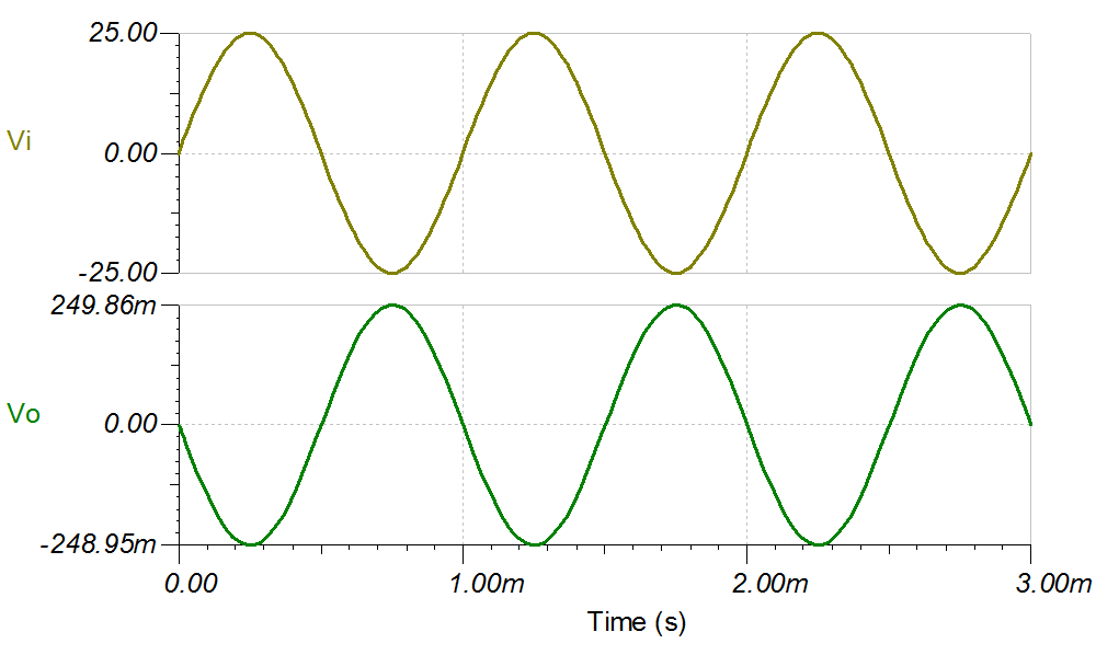
Transient Simulation Results

Design References
Texas Instruments, Simulation for Band Pass Filtered Inverting Attenuator Circuit, circuit SPICE simulation file
Texas Instruments, Bandpass-Filtered -40-DB Attenuator, Less than 0.1-DB Error, reference design
Design Featured Op Amp
| OPA1612 | |
|---|---|
| Vss | 4.5V to 36V |
| VinCM | Vee+2V to Vcc–2V |
| Vout | Vee+0.2V to Vcc–0.2V |
| Vos | 100µV |
| Iq | 3.6mA/Ch |
| Ib | 60nA |
| UGBW | 40MHz |
| SR | 27V/µs |
| #Channels | 1 and 2 |
| OPA1612 | |
Design Alternate Op Amp
| OPA172 | |
|---|---|
| Vss | 4.5V to 36V |
| VinCM | Vee–100mV to Vcc–2V |
| Vout | Rail-to-rail |
| Vos | 200µV |
| Iq | 1.6mA/Ch |
| Ib | 8pA |
| UGBW | 10MHz |
| SR | 10V/µs |
| #Channels | 1, 2, and 4 |
| OPA172 | |