SBOA217B January 2018 – October 2024 OPA197 , TLV172
Design Goals
| Input | Output | Supply | ||||
|---|---|---|---|---|---|---|
| ViMin | ViMax | VoMin | VoMax | Vcc | Vee | Vref |
| ±25mV | ±10V | 25mV | 10V | 15V | –15V | 0V |
Design Description
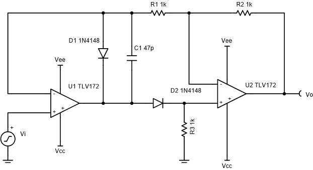
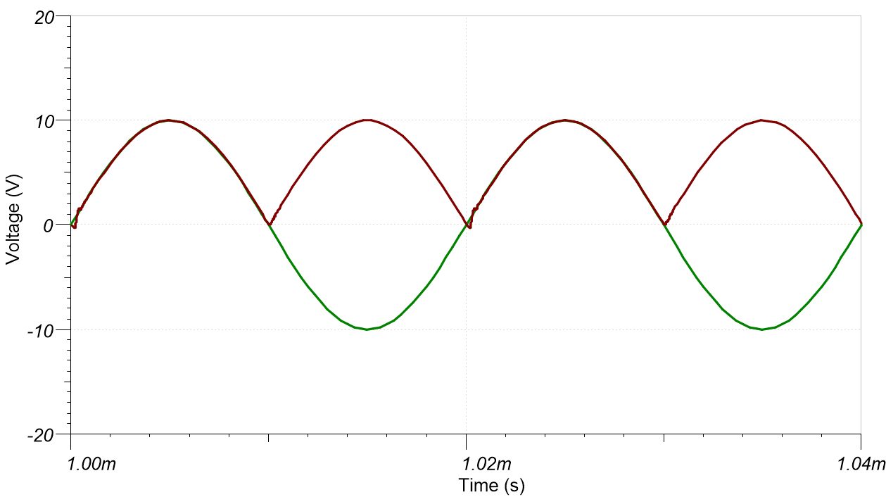
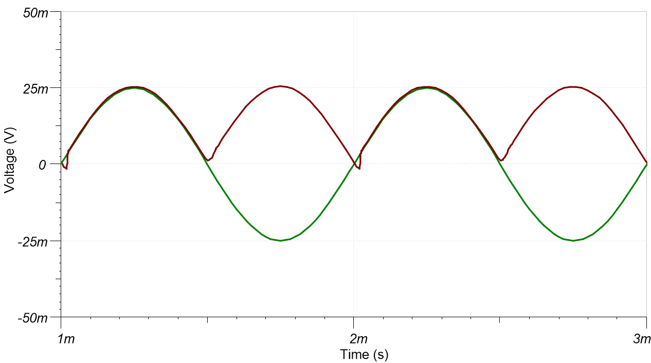
This absolute value circuit can turn alternating current (AC) signals to single polarity signals. This circuit functions with limited distortion for ±10V input signals at frequencies up to 50kHz and for signals as small as ±25mV at frequencies up to 1kHz.

Design Notes
- Be sure to select an op amp with sufficient bandwidth and a high slew rate.
- For greater precision look for an op amp with low offset voltage, low noise, and low total harmonic distortion (THD).
- The resistors were selected to be 0.1% tolerance to reduce gain error.
- Selecting too large of a capacitor C1 causes large distortion on the transition edges when the input signal changes polarity. C1 may not be required for all op amps.
- Use a fast switching diode.
Design Steps
- Select gain resistors.
- Gain for positive input
signals.
- Gain for negative input signals.
- Gain for positive input
signals.
- Select R1 and
R2 to reduce thermal noise and to minimize voltage drops due to
the reverse leakage current of the diode. These resistors will appear as loads
to U1 and U2 during negative input signals.
- R3 biases the
non-inverting node of U2 to GND during negative input signals. Select
R3 to be the same value as R1 and R2.
U1 must be able to drive the R3 load during positive
input signals.
- Select C1 based on the desired transient response. See the Design Reference section for more information.
Design Simulations
Transient Simulation Results
 ±10V at 50kHz Input
 ±25mV at 1kHz Input
Design References
Texas Instruments, Simulation for Photodiode Amplifier, circuit SPICE simulation file
Texas Instruments, Prevision Full-Wave Rectifier, Dual-Supply, reference design
Design Featured Op Amp
| TLV172 | |
|---|---|
| Vcc | 4.5V to 36V |
| VinCM | Vee to (Vcc–2V) |
| Vout | Rail-to-rail |
| Vos | 0.5mV |
| Iq | 1.6mA/Ch |
| Ib | 10pA |
| UGBW | 10MHz |
| SR | 10V/µs |
| #Channels | 1, 2, and 4 |
| TLV172 | |
Design Alternate Op Amp
| OPA197 | |
|---|---|
| Vcc | 4.5V to 36V |
| VinCM | Rail-to-rail |
| Vout | Rail-to-rail |
| Vos | 25µV |
| Iq | 1mA/Ch |
| Ib | 5pA |
| UGBW | 10MHz |
| SR | 20V/µs |
| #Channels | 1, 2, and 4 |
| OPA197 | |