SBOA234A January 2019 – October 2024 OPA140 , OPA376
Design Goals
| Input | Output | Supply | |||||
|---|---|---|---|---|---|---|---|
| ViMin | ViMax | VoMin | VoMax | Vcc | Vee | Vdd | Vref |
| –10V | +10V | +0.2V | +4.8V | +15V | –15V | +5V | +4.096V |
Design Description
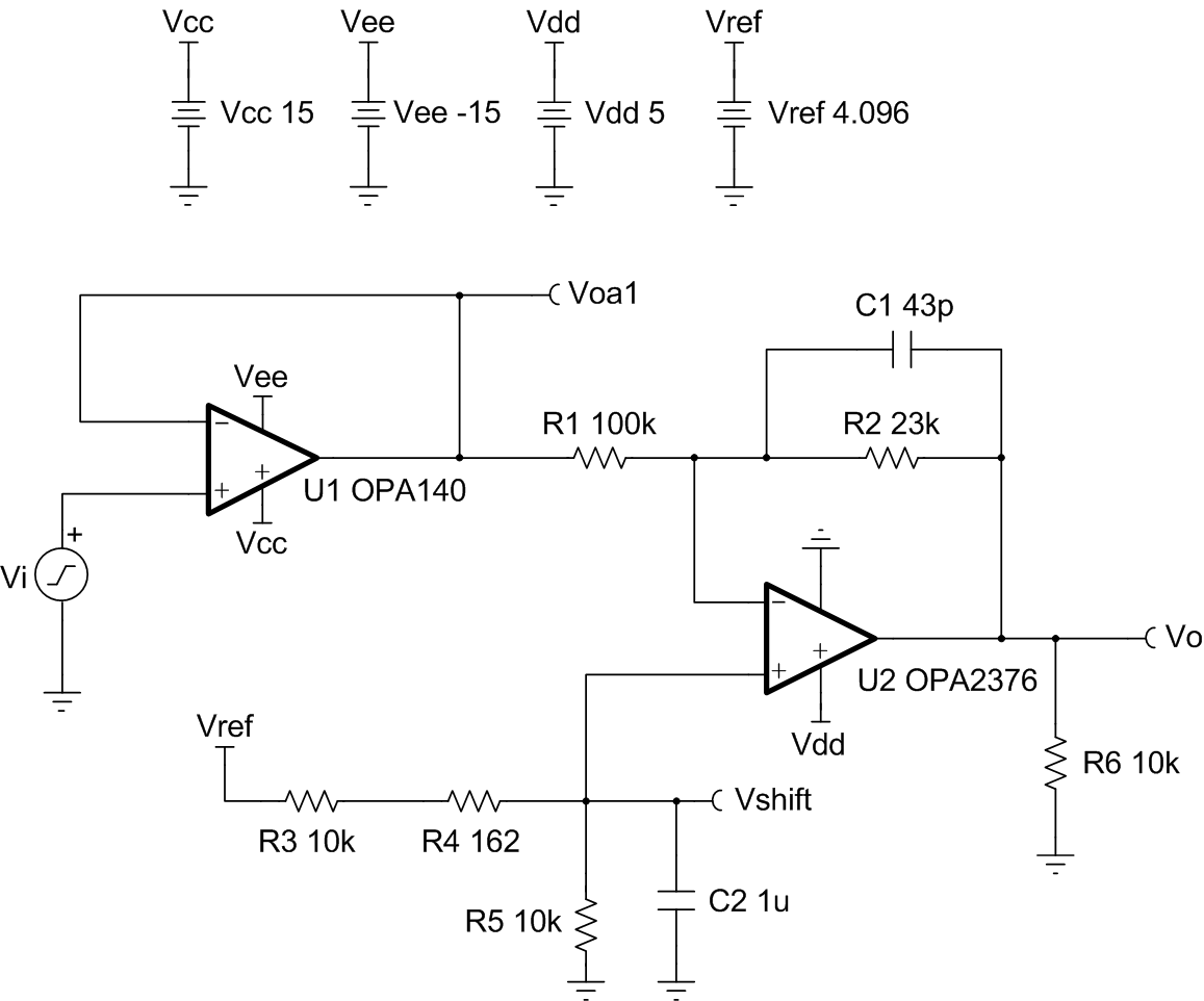
This inverting dual-supply to single-supply amplifier translates a ±10V signal to a 0V to 5V signal for use with an ADC. Levels can easily be adjusted using the given equations. The buffer can be replaced with other ±15V configurations to accommodate the desired input signal, as long as the output of the first stage is low impedance.

Design Notes
- Observe common-mode limitations of the input buffer.
- A high-impedance source will alter the gain characteristics of U2 if buffer amplifier U1 is not used.
- R6 provides a path to ground for the output of U1 if the ±15V supplies come up before the 5V supply. This limits the voltage at the inverting pin of U2 through the voltage divider created by R1, R2, and R6 and prevents damage to U2 as well as to any converter that may be connected to its output. To best protect the devices a transient voltage suppressor (TVS) should be used at the power pins of U2.
- A capacitor across R5 will help filter Vref and provide a cleaner Vshift.
Design Steps
The transfer function for this circuit follows:
- Set the gain of the amplifier.
- Set Vshift to translate
the signal to single supply.
- Select resistors for reference
voltage divider to achieve Vshift.
- Large
feedback resistors can interact with the input capacitance and cause
instability. Choose C1 to add a pole to the transfer function to
counteract this. The pole must be lower in frequency than the effective
bandwidth of the op amp.
Design Simulations
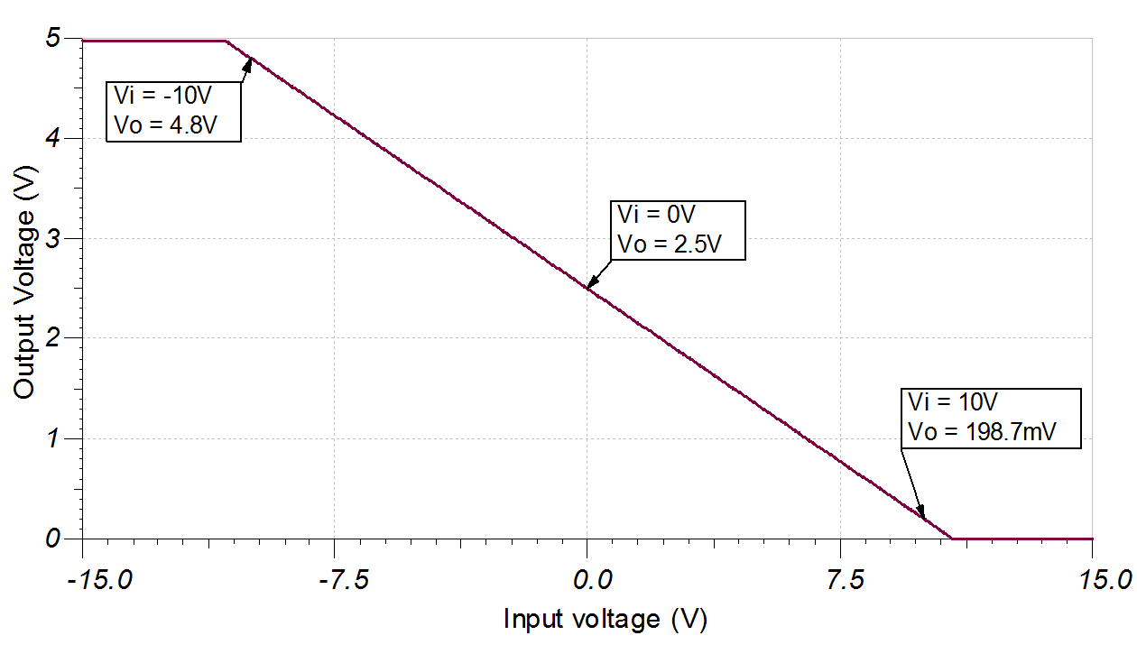
DC Simulation Results

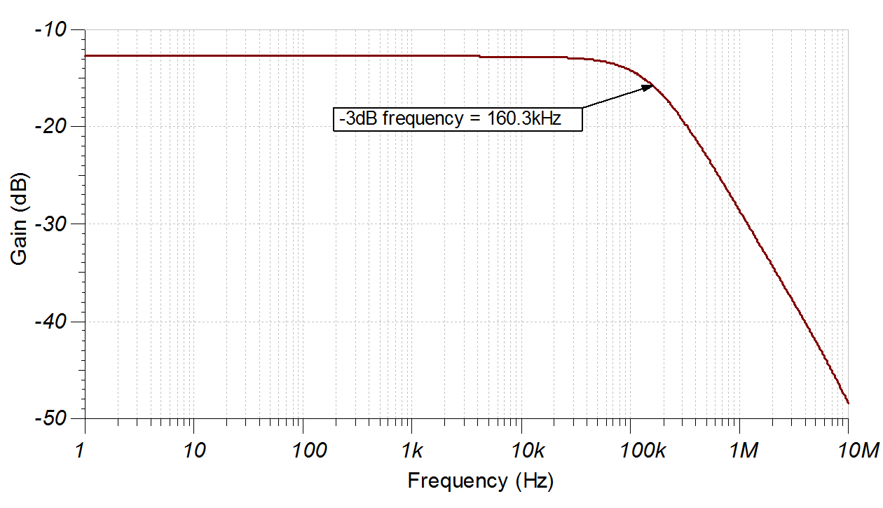
AC Simulation Results

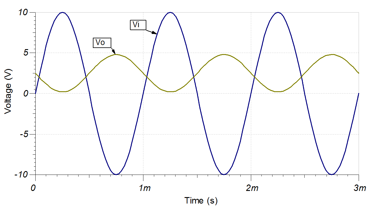
Transient Simulation Results

Design References
Texas Instruments, SBOMAT9 TINA-TI™ circuit simulation, file download
Texas Instruments, TIPD148 Level Translation: Dual to Single Supply Amp, ±15V to 5V, product page
Design Featured Op Amp
| OPA376 | |
|---|---|
| Vss | 2.2V to 5.5V |
| VinCM | Vee to Vcc-1.3 V |
| Vout | Rail-to-rail |
| Vos | 5µV |
| Iq | 760 µA/Ch |
| Ib | 0.2pA |
| UGBW | 5.5MHz |
| SR | 2V/µs |
| #Channels | 1, 2, and 4 |
| OPA376 | |
Design Featured Op Amp
| OPA140 | |
|---|---|
| Vss | 4.5V to 36V |
| VinCM | Vee-0.1V to Vcc-3.5V |
| Vout | Rail-to-rail |
| Vos | 30µV |
| Iq | 1.8mA/Ch |
| Ib | ±0.5pA |
| UGBW | 11MHz |
| SR | 20V/µs |
| #Channels | 1, 2, and 4 |
| OPA140 | |