SBOA244A January 2019 – October 2024 OPA827 , TLC072
Design Goals
| Input | Output | Supply | |||
|---|---|---|---|---|---|
| ViMin | ViMax | VoMin | VoMax | Vcc | Vee |
| –12V | 12V | –12V | 12V | 15V | –15V |
| Cutoff Frequency (fc) | Diode Threshold Voltage (Vt) |
|---|---|
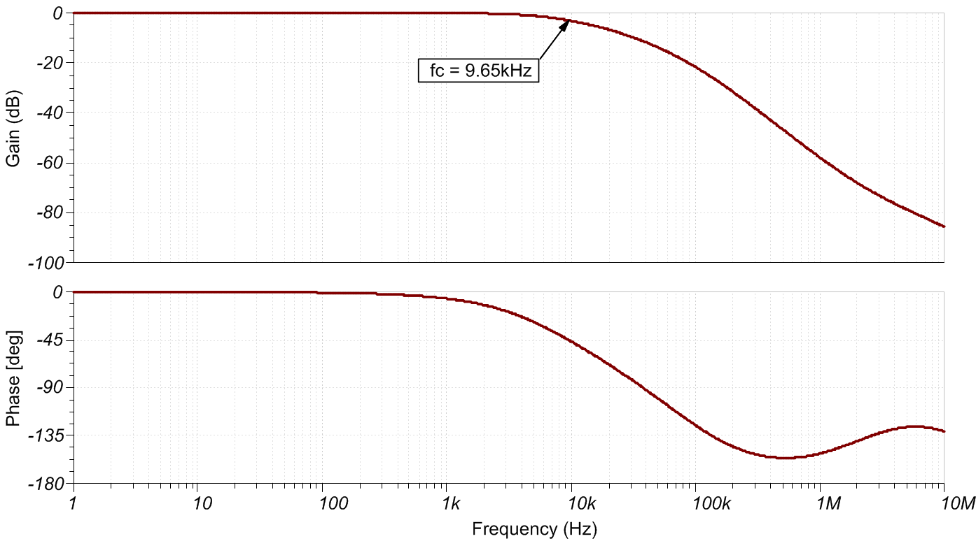
| 10kHz | 20mV |
Design Description
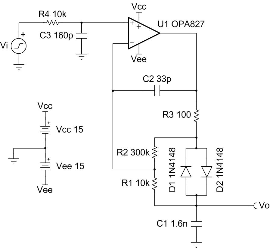
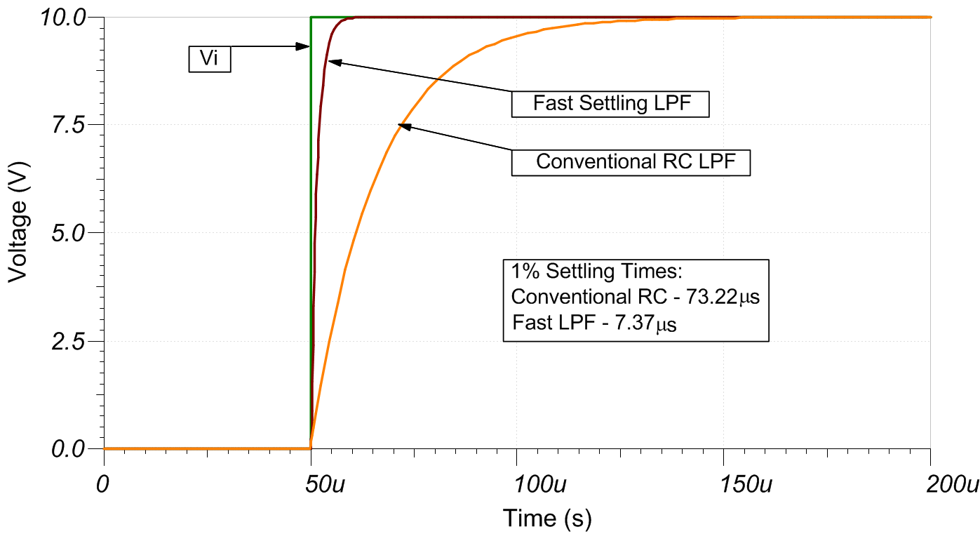
This low-pass filter topology offers a significant improvement in settling time over the conventional single-pole RC filter. This is achieved through the use of diodes D1 and D2, that allow the filter capacitor to charge and discharge much faster when there is a large enough difference between the input and output voltages.

Design Notes
- Observe the common-mode input limitations of the op amp.
- Keeping C1 small will ensure the op amp does not struggle to drive the capacitive load.
- For the fastest settling time, use fast switching diodes.
- The selected op amp should have sufficient output drive capability to charge C1. R3 limits the maximum charge current.
Design Steps
- Select standard values for
R1 and C1 based on fC = 10kHz.
- Set the diode threshold voltage
(Vt). This threshold is the minimum difference in voltage between
the input and output that will result in diode conduction (fast capacitor
charging and discharging).
- Select components for noise
pre-filtering.
- Add compensation components to
stabilize U1. R3 limits the charge current into
C1 and also serves to isolate the capacitance from the op amp
output when the diodes are conducting. Larger values will improve stability but
increase C1 charge time.
- C2 provides local high
frequency feedback to counteract the interaction between the input capacitance
with the parallel combination of R1 and R2. To prevent
interaction with C1, select C2 as the following shows:
Design Simulations
AC Simulation Results

Transient Simulation Results

Design References
Texas Instruments, SBOMAU1 TINA-TI™ circuit simulation, file download
Design Featured Op Amp
| OPA827 | |
|---|---|
| Vss | 8V to 36V |
| VinCM | Vee+3V to Vcc–3V |
| Vout | Vee+3V to Vcc–3V |
| Vos | 75µV |
| Iq | 4.8mA |
| Ib | 3pA |
| UGBW | 22MHz |
| SR | 28V/µs |
| #Channels | 1 |
| OPA827 | |
Design Alternate Op Amp
| TLC072 | |
|---|---|
| Vss | 4.5V to 16V |
| VinCM | Vee+0.5V to Vcc–0.8V |
| Vout | Vee+350mV to Vcc–1V |
| Vos | 390µV |
| Iq | 2.1mA/Ch |
| Ib | 1.5pA |
| UGBW | 10MHz |
| SR | 16V/µs |
| #Channels | 1, 2, and 4 |
| TLC072 | |