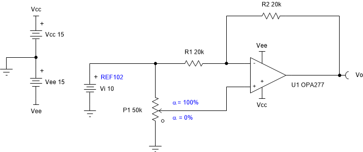
Adjustable Reference Voltage Circuit
Design Goals
| Input | Output | Supply | ||
|---|---|---|---|---|
| Vi | VoMin | VoMax | Vcc | Vee |
| 10V | –10V | 10V | 15V | –15V |
Design Description
This circuit combines an inverting and non-inverting amplifier to make a reference voltage adjustable from the negative of the input voltage up to the input voltage. Gain can be added to increase the maximum negative reference level.
Design Notes
- Observe the common-mode and output swing limitations of the op amp.
- Mismatch in R1 and R2 results in a gain error. Selecting R2 > R1 increases the maximum negative voltage, and selecting R2 < R1 decreases the maximum negative voltage. In either case, the maximum positive voltage is always equal to the input voltage. This relationship is inverted if a negative input reference voltage is used.
- Select the potentiometer based on the desired resolution of the reference. Generally, the potentiometers can be set accurately to within one-eighth of a turn. For a 10-turn pot this means alpha (∝) may be off by as much as 1.25%.
Design Steps
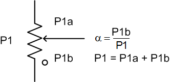
Alpha represents the potentiometer setting relative to ground. This is the fraction of the input voltage that will be applied to the non-inverting terminal of the op amp and amplified by the non-inverting gain.
The transfer function of this circuit follows:
- If R2 = R1 =
20kΩ, then the equation for Vo simplifies as the following shows:
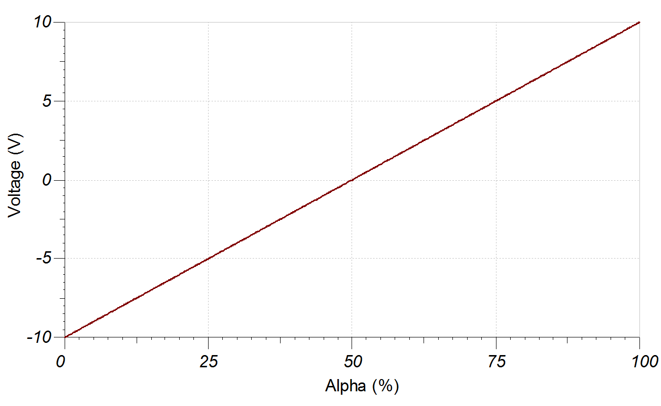
- If Vi = 10V and ∝ =
0.75, the value of Vo can be determined.
Design Simulations
DC Simulation Results
Design References
Texas Instruments, SBOMAU2 TINA-TI™ circuit simulation, file download
Design Featured Op Amp
| OPA277 | |
|---|---|
| Vss | 4V to 36V |
| VinCM | Vee+2V to Vcc–2V |
| Vout | Vee+0.5V to Vcc–1.2V |
| Vos | 10µV |
| Iq | 790µA/Ch |
| Ib | 500pA |
| UGBW | 1MHz |
| SR | 0.8V/µs |
| #Channels | 1, 2, and 4 |
| OPA277 | |
Design Alternate Op Amp
| OPA172 | |
|---|---|
| Vss | 4.5V to 36V |
| VinCM | Vee–0.1V to Vcc–2V |
| Vout | Rail-to-rail |
| Vos | 200µV |
| Iq | 1.6 mA/Ch |
| Ib | 8pA |
| UGBW | 10MHz |
| SR | 10V/µs |
| #Channels | 1, 2, and 4 |
| OPA172 | |
Trademarks
All trademarks are the property of their respective owners.