SBOA269B February 2018 – September 2024 LM7332 , OPA192
Design Goals
| Input | Output | Freq. | Supply | |||
|---|---|---|---|---|---|---|
| ViMin | ViMax | VoMin | VoMax | f | Vcc | Vee |
| –10V | 10V | –10V | 10V | 100kHz | 15V | –15V |
Design Description
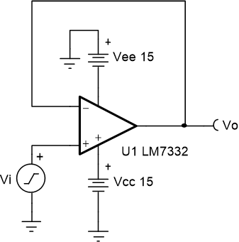
This design is used to buffer signals by presenting a high input impedance and a low output impedance. This circuit is commonly used to drive low-impedance loads, analog-to-digital converters (ADC) and buffer reference voltages. The output voltage of this circuit is equal to the input voltage.

Design Notes
- Use the op-amp linear output operating range, which is usually specified under the AOL test conditions.
- The small-signal bandwidth is determined by the unity-gain bandwidth of the amplifier.
- Check the maximum output voltage swing versus frequency graph in the data sheet to minimize slew-induced distortion.
- The common mode voltage is equal to the input signal.
- Do not place capacitive loads directly on the output that are greater than the values recommended in the data sheet.
- High output current amplifiers may be required if driving low impedance loads.
- For more information on op-amp linear operating region, stability, slew-induced distortion, capacitive load drive, driving ADCs, and bandwidth, see the Design References section.
Design Steps
The transfer function for this circuit follows:
- Verify that the amplifier can achieve the
desired output swing using the supply voltages provided. Use the output swing stated in
the AOL test conditions. The output swing range of the amplifier must be
greater than the output swing required for the design.
- The output swing of the LM7332 using ±15V supplies is greater than the required output swing of the design. Therefore, this requirement is met.
- Review the Output Voltage versus Output Current curves in the product data sheet to verify the desired output voltage can be achieved for the desired output current.
- Verify the input common mode voltage of the
amplifier is not violated using the supply voltage provided. The input common mode voltage
range of the amplifier must be greater than the input signal voltage range.
- The input common-mode range of the LM7332 using ±15V supplies is greater than the required input common-mode range of the design. Therefore, this requirement is met.
- Calculate the minimum slew rate required to
minimize slew-induced distortion.
- The slew rate of the LM7332 is 15.2 V/µs. Therefore, this requirement is met.
- Verify the device has sufficient bandwidth
for the desired output signal frequency.
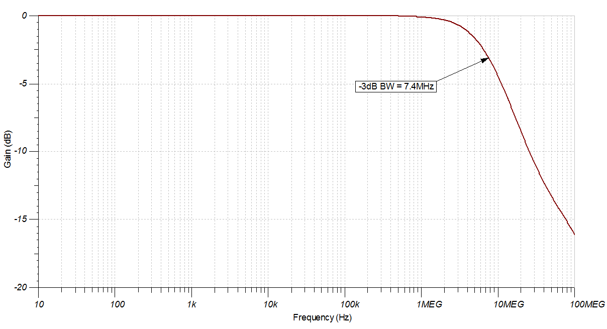
- The desired output signal frequency is less than the unity-gain bandwidth of the LM7332. Therefore, this requirement is met.
Design Simulations
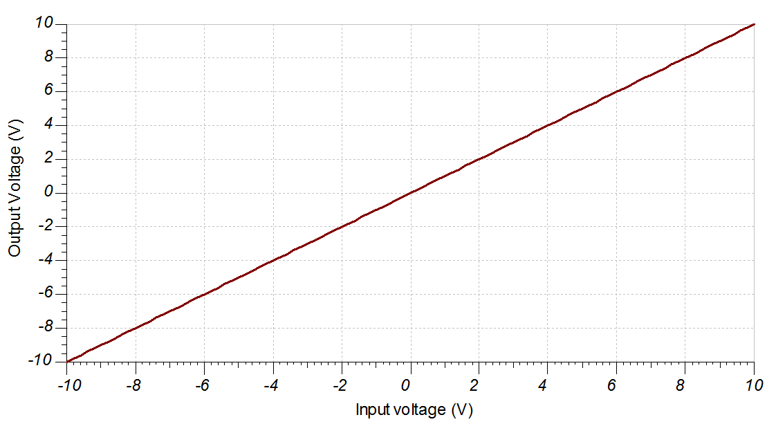
DC Simulation Results

AC Simulation Results

Design References
Texas Instruments, Capacitive Load Drive Verified Reference Design Using an Isolation Resistor, TIPD128 verified design
Texas Instruments, Simulation for Buffer (Follower) Circuit, SBOC491 software tool
Design Featured Op Amp
| LM7332 | |
|---|---|
| Vss | 2.5V to 32V |
| VinCM | Rail-to-rail |
| Vout | Rail-to-rail |
| Vos | 1.6mV |
| Iq | 2mA |
| Ib | 1µA |
| UGBW | 7.5MHz (±5V supply) |
| SR | 15.2V/µs |
| #Channels | 2 |
| LM7332 | |
Design Alternate Op Amp
| OPA192 | |
|---|---|
| Vss | 4.5V to 36V |
| VinCM | Rail-to-rail |
| Vout | Rail-to-rail |
| Vos | 5µV |
| Iq | 1mA |
| Ib | 5pA |
| UGBW | 10MHz |
| SR | 20V/µs |
| #Channels | 1, 2, and 4 |
| OPA192 | |
The following device is for battery-operated or power-conscious designs outside of the original design goals described earlier, where lowering the total system power is desired.
| LPV511 | |
|---|---|
| Vss | 2.7V to 12V |
| VinCM | Rail-to-rail |
| Vout | Rail-to-rail |
| Vos | 0.2mV |
| Iq | 1.2µA |
| Ib | 0.8nA |
| UGBW | 27KHz |
| SR | 7.5V/ms |
| #Channels | 1 |
| LPV511 | |