SBOA281 december 2018 OPA172 , TLV171
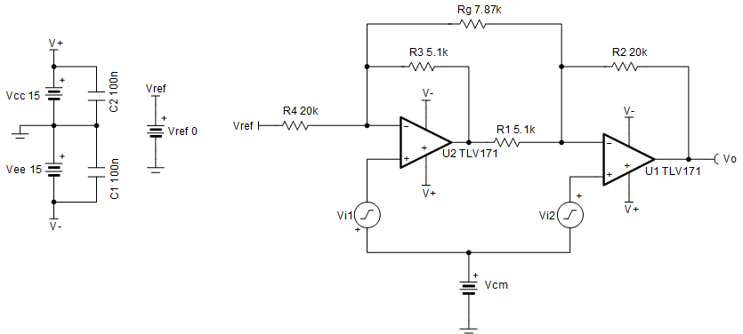
Design Goals
| Input ViDiff(Vi2 - Vi1) | Output | Supply | ||||
|---|---|---|---|---|---|---|
| ViDiff_Min | ViDiff_Max | VoMin | VoMax | Vcc | Vee | Vref |
| +/–1V | +/–2V | –10V | +10V | 15V | –15V | 0V |
| Vcm | Gain Range |
|---|---|
| +/-10V | 5V/V to 10V/V |
Design Description
This design amplifiers the difference between Vi1 and Vi2 and outputs a single ended signal while rejecting the common–mode voltage. Linear operation of an instrumentation amplifier depends upon the linear operation of its primary building block: op amps. An op amp operates linearly when the input and output signals are within the device’s input common–mode and output–swing ranges, respectively. The supply voltages used to power the op amps define these ranges.
Design Notes
- Rg sets the gain of the circuit.
- High–value resistors can degrade the phase margin of the circuit and introduce additional noise in the circuit.
- The ratio of R4 and R3 set the minimum gain when Rg is removed.
- Ratios of R2/R1 and R4/R3 must be matched to avoid degrading the instrumentation amplifier’s DC CMRR and ensuring the Vref gain is 1V/V.
- Linear operation is contingent upon the input common–mode and the output swing ranges of the discrete op amps used. The linear output swing ranges are specified under the Aol test conditions in the op amps data sheets.
Design Steps
- Transfer function of this circuit.
- Select R4 and
R3 to set the minimum gain.
- Select R1 and
R2. Ensure that R1/R2 and
R3/R4 ratios are matched to set the gain applied to
the reference voltage at 1V/V.
- Select Rg to meet the desired maximum gain G = 10V/V.
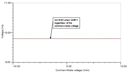
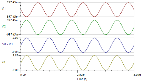
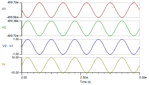
Design Simulations
DC Simulation Results
Transient Simulation Results
References:
- Analog Engineer's Circuit Cookbooks
- SPICE Simulation File SBOMAU7
- TI Precision Labs
- VCM vs. VOUT plots for instrumentation amplifiers with two op amps
- Common-mode Range Calculator for Instrumentation Amplifiers
| TLV171 | |
|---|---|
| Vss | 4.5V to 36V |
| VinCM | (Vee–0.1V) to (Vcc–2V) |
| Vout | Rail–to–rail |
| Vos | 0.25mV |
| Iq | 475µA |
| Ib | 8pA |
| UGBW | 3MHz |
| SR | 1.5V/µs |
| #Channels | 1,2,4 |
| www.ti.com/product/tlv171 | |
Design Alternate Op Amp
| OPA172 | |
|---|---|
| Vss | 4.5V to 36V |
| VinCM | (Vee–0.1V) to (Vcc–2V) |
| Vout | Rail–to–rail |
| Vos | 0.2mV |
| Iq | 1.6mA |
| Ib | 8pA |
| UGBW | 10MHz |
| SR | 10V/µs |
| #Channels | 1,2,4 |
| www.ti.com/product/opa172 | |