SBOA336A January 2019 – September 2024 INA186 , INA186-Q1 , INA190 , INA190-Q1
| Input | Output | Supply | Temperature | ||||||
|---|---|---|---|---|---|---|---|---|---|
| Iload Min | Iload Max | VCM | VOUT Min | VOUT Max | IQ Max | VVS | Vee | Low | High |
| 1µA | 104 µA | –0.1V ≤ VCM ≤ 40V | 31.0mV at 1µA | 3.224V at 104µA | 65µA | 3.3V | GND (0V) | 0°C | 85°C |
Design Description
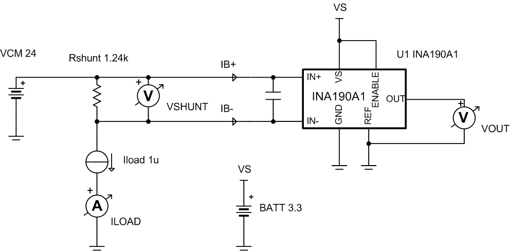
This circuit demonstrates how to use a current sense amplifier to accurately and robustly measure small micro-amp currents and maximize dynamic range. The following error analysis can be applied to many current sense amplifiers. This design relies on using a precision, low input-bias current sense amplifier and analyzing the dynamic error due to input bias currents on large shunt resistors.
Design Notes
- The Getting Started with Current Sense Amplifiers video series introduces implementation, error sources, and advanced topic for using current sense amplifiers.
- Choose a precision 0.1% shunt resistor to limit gain error at higher currents.
- Choose a low input-bias current (high input-impedance) amplifier such as the INA190.
- Confirm VCM is within the operating VCM range of INA190: –0.1V to 40V.
- Error significantly reduces if DC offsets are calibrated out with one-point calibration or if device operates under the same conditions as the INA190 Low-Supply, High-Accuracy, Low- and High-Side Current-Shunt Monitor With Picoamp Bias Current and Enable data sheet specifies (VVS = 1.8V, VCM = 12V, VREF = 0.9V, TA = 25°C). A two-point calibration can be done to eliminate gain error.
- It is recommended to add ≥ 1nF input differential capacitor to INA190 inputs when working with large shunt resistors and DC currents.
- Follow best practices for layout according to the data sheet: decoupling capacitor close to VS pin, routing the input traces for IN+ and IN- as a differential pair, and so forth.
Design Steps
- Given the design requirements,
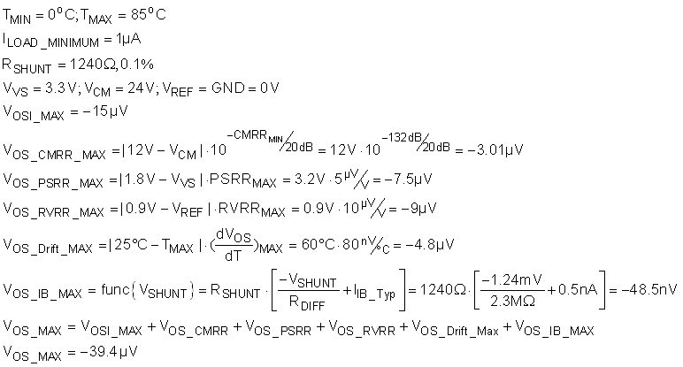
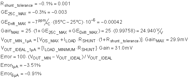
verify the shunt resistor achieves a maximum total error of 3.51% at 1µA load
current. Assume all offset and gain errors are negative. Note that error due to
input bias current (IIB) is a function of the VSHUNT and
input differential impedance (RDIFF) where RDIFF =
IIB+/VDIFF. Since IIB- starts around +500
pA and decreases as VSHUNT increases, this generates a negative input
offset error. See the IB+ and IB- vs Differential Input Voltage plot in
the data sheet.
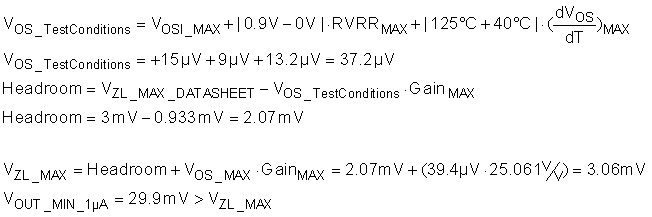
- Verify that the sensed current range fits within the output
dynamic range of the device. This depends upon two specifications:
Swing-to-VVS (VSP) and Zero-current Output Voltage
(VZL). VZL is specified over -40°C to +125°C at
VVS = 1.8V, VREF = 0V, VSENSE = 0mV,
VCM = 12V, and RL = 10kΩ. Since data sheet conditions
do not match the conditions of this design, extrapolate what the maximum
VZL would be.
- Calculate the maximum possible positive offset for testing conditions of VZL. Call this VOS_TestConditions.
- Convert this input offset into an output offset by multiplying by maximum possible gain.
- Determine the Headroom voltage by taking difference between the VZL_MAX from data sheet and the previously determined maximum output offset.
- Calculate VZL_MAX in this design by adding the Headroom voltage to the maximum possible output offset for this design.
- Verify that the minimum
VOUT at 1µA is greater than VZL_MAX. Note
VOUT_MIN at 1µA assumes worst-case scenario of –1%
tolerance for RSHUNT and negative input offsets.
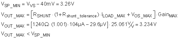
- Now establish that the
maximum VOUT at 104µA is less than VSP_MIN. Note
VOUT_MAX at 104µA assumes worst-case scenario of +1%
tolerance for RSHUNT and positive input offsets.
- Generate Total Error vs Load Current curves based upon the total error equations in Step 1. Do this for the typical and maximum data sheet specifications.
Design Simulations
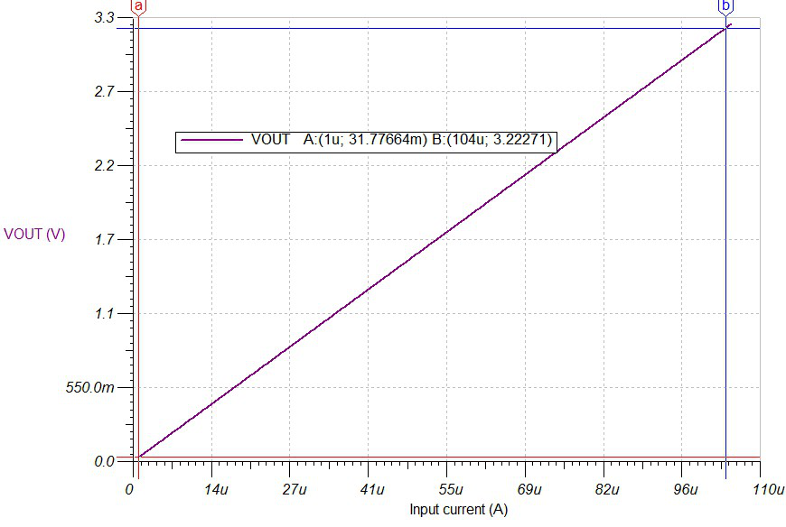
DC Simulation Results
The following graph shows a linear output response for load currents from 1µA to 104µA
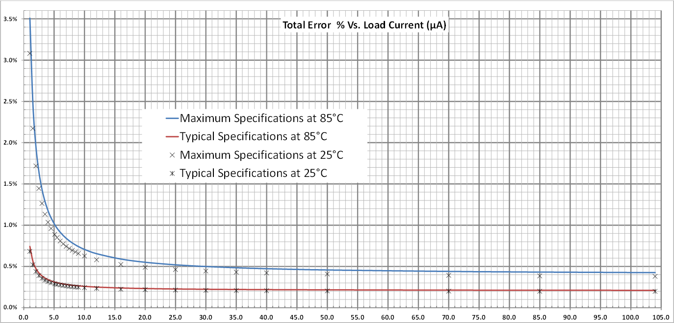
Total Error Calculations
The following graph shows the total absolute error over temperature using both the assured limit specifications and the typical specifications. Note that accuracy is limited by the offset voltage at the lowest current sensed and limited by gain error at higher currents. Active offset chopping limits the error due to temperature.
Design References
Texas Instruments, SBOMAI6 circuit SPICE, simulation file
Texas Instruments, Getting started with current sense amplifiers, Precision labs video series
Texas Instruments, Extending the Common-Mode Voltage Range of Current-Output Current Shunt Monitors, application brief
Texas Instruments, Current sense amplifiers, products page
Design Featured Current Shunt Monitor
| INA190A1 | ||||
|---|---|---|---|---|
| VVS | 1.8V to 5V (operating) | |||
| VCM | -0.3V to 42V (survivability) | |||
| VOUT | Up to (VVS) + 0.3V | |||
| VOS | ±3µV to ±15µV | |||
| IQ | 48µA to 65µA | |||
| IIB | 0.5nA to 3nA | |||
| BW | 45kHz at 25V/V (A1 gain variant) | |||
| # of Channels | 1 | |||
| INA190 | ||||