SBOA510 March 2021 OPA455 , OPA462
- Trademarks
- 1Introduction
- 2Three Op Amp OPA462 HV Solution
- 3Lower Voltage, Lower Cost Three Op Amp Solution
- 4OPA462 300 Vpp Output Solution With Discrete Transistor Supply-Rail Drivers
- 5Lessons Learned from the Practical Implementation of the HV Op Amp Solutions
-
A Appendix
- A.1 Overview
- A.2 Summary of Results
- A.3 Test Setup and Equipment
- A.4 Printed Circuit Boards
- A.5 Power Supply, Source Measurement Unit (SMU)
- A.6 Arbitrary Waveform Generator (AWG)
- A.7 Oscilloscope
- A.8 Circuit 1: OPA462 Three op amp Solution
- A.9 Circuit 2: Lower Voltage, Lower Cost Three Op Amp Solution
- A.10 Circuit 3: OPA462 300 Vpp Output Solution With Discrete Transistor Supply-Rail Drivers
A.8.3 Results
 Figure 6-4 Noninverting Configuration, G =
+66 V/V, 1-kHz Sine Wave (Output 344 Vpp)
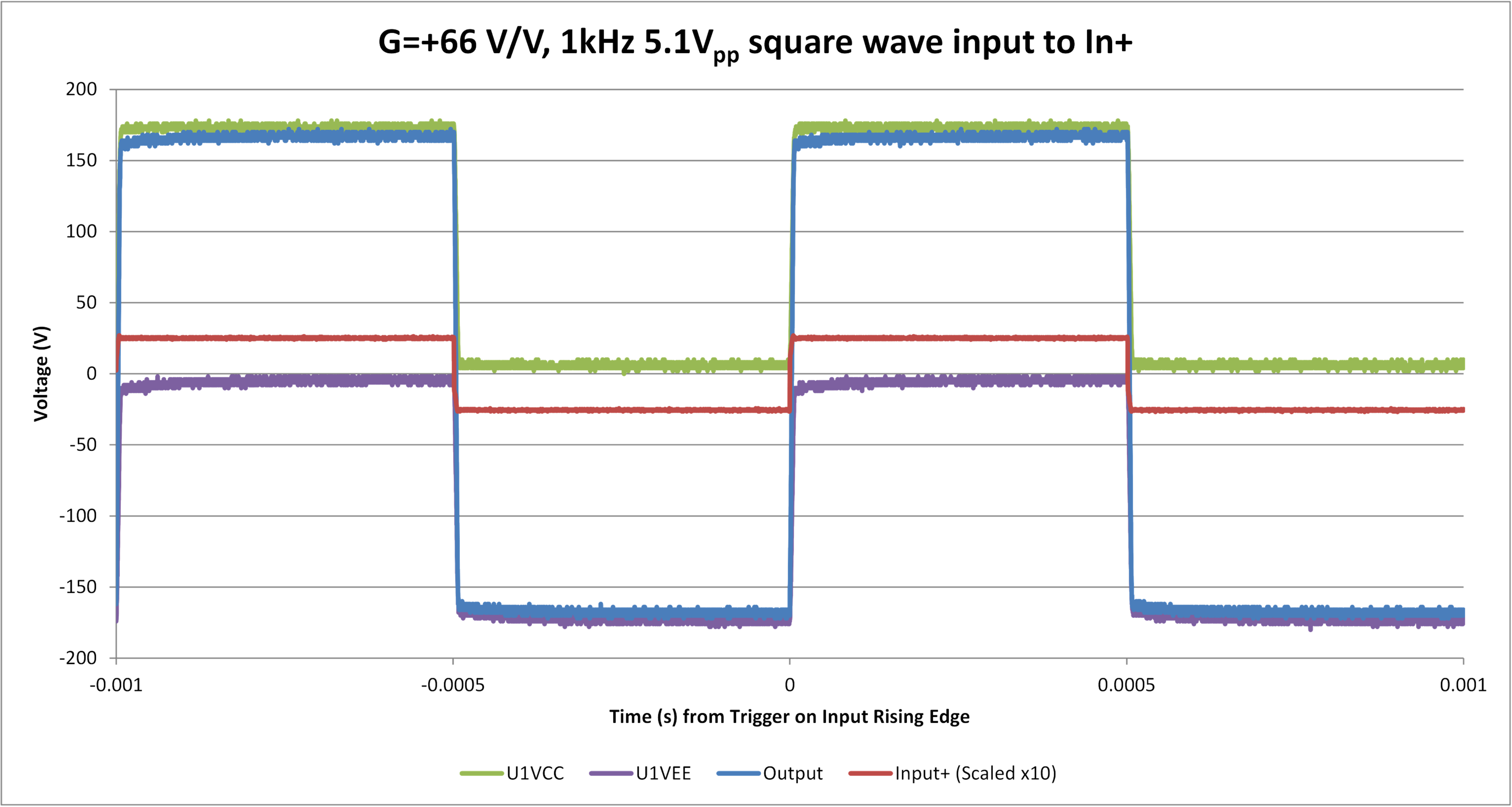
 Figure 6-5 Noninverting Configuration, G =
+66 V/V, 1-kHz Square Wave (Output 344 Vpp)
Figure 6-5 Noninverting Configuration, G =
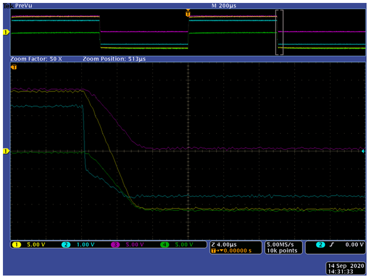
+66 V/V, 1-kHz Square Wave (Output 344 Vpp)Figure 6-6 and Figure 6-7 show the falling and rising edges of the above square wave waveform, but at a higher zoom level. Please note that the actual values of Channels 1, 3, and 4 are 10 × greater than the image implies, due to the attenuation settings of the scope probes.
 Figure 6-6 Noninverting Configuration, G = 66
V/V, 1-kHz Square Wave (5.1 Vpp), Zoom on Falling Edge
 Figure 6-7 Noninverting Configuration, G =
+66 V/V, 1-kHz Square Wave (5.1 Vpp), Zoom on Rising Edge