Build a Programmable Gain Transimpedance Amplifier Using the OPA3S328
Trademarks
All trademarks are the property of their respective owners.
1 Introduction
Photodiode sensors produce a current output that changes with incident light, where the typical photocurrent changes orders of magnitude from hundreds of pico-amps to a few milliamps. Transimpedance amplifiers are essential circuits in photodiode acquisition systems to convert photocurrent to voltage that will drive a typical Analog-to-Digital (ADC) converter.
TIAs are required to amplify a photodiode's signal while meeting low-noise, high-resolution, and high-bandwidth constraints. A programmable gain TIA stage allows flexibility to measure the wide range of photodiode current while ensuring the amplifier remains inside its linear range. Programmable gain TIAs are essential in many systems. Applications include photosensor devices such as chemical analysis systems, infrared spectroscopes, data acquisition systems and optical communication applications where the optical power in a fiber can vary widely, and, as a result yield wide current ranges from an optical detector.
The OPA3S328 is a dual precision CMOS operational amplifier (op-amp) with integrated switches optimized for programmable gain transimpedance amplifier applications. The dual op-amp offers low input bias current, DC precision performance, low noise, high bandwidth, providing an optimal choice for transimpedance amplifier applications.
The simplified circuit diagram shown in Figure 1-1 shows a programmable gain TIA circuit implemented with the OPA3S328. The OPA3S328 integrates analog switches useful to select the TIA gains across multiple decades of photodiode current. The second-stage amplifier buffers the programmable gain TIA stage using Kelvin sense connections to eliminate errors due to the switch on-resistance, switch resistance drift, and non-linearity. This document provides a step-by-step example for designing a low noise, high bandwidth, high accuracy programmable TIA to perform optical power measurements using a near infrared (NIR) wavelength photodiode.
 Figure 1-1 Switched Gain Transimpedance Amplifier
2 The Transimpedance Amplifier and Photodiode Sensor
A transimpedance amplifier consists of an op amp and a feedback resistor. The photosensor current to be amplified is applied to the inverting input, causing the output voltage of the amplifier to change, as shown in Figure 2-1:
 Figure 2-1 Photodiode Transimpedance Amplifier
The feedback resistor (RF) across the op amp converts the photodiode current (ID) to a voltage (VOUT) using Ohm’s law, as shown in Equation 12.
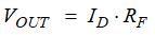
The feedback resistor (RF) determines the gain of the transimpedance op-amp. For the transimpedance current to voltage conversion to be accurate, the amplifier’s input bias current and input offset voltage must be small. The OPA3S328 offers low offset voltage, 25µV (max) and low input bias current, 0.2 pA. The photodiode parasitic junction capacitance plays a significant role in the stability and bandwidth of the TIA circuit, as we will discuss in detail in the following sections. The feedback capacitor (CF) is required to compensate the circuit for stability.
This example shows a large area near-infrared (NIR) wavelength Indium Gallium Arsenide (InGaAs) photodiode for the design. In this specific application, the photodiode operates on the photoconductive mode, where exposure to light causes a reverse current through the detector. A reverse bias is applied to the photosensor to reduce the junction capacitance. The reverse bias voltage (VR) dramatically improves the speed of response and linearity of the photodiode. The reverse bias increases the depletion region width and consequently decreases the junction capacitance. The dark current of this photosensor is about 50nA in this mode of operation. Table 2-1 shows the photodiode parameters.
| Parameter | Symbol | Value | Unit |
|---|---|---|---|
| Reverse Voltage | VR | -3 | V |
| Junction Capacitance (VR=-3V) | CJ | 100 | pF |
| Reverse Current Range | ID | 0-2000 | µA |
| Dark Current | Idark | 50 | nA |
There are different ways to bias the photodiode in the TIA circuit. A common method used on unipolar supply applications is to bias the op-amp non-inverting input (+IN) with a positive dc voltage. The positive voltage at the non-inverting input will reverse bias the photodiode while allowing the amplifier output to reach true zero when the photodiode is unexposed to light and respond without the added delay that results from coming out of the negative rail. Figure 2-2 shows a typical way to reverse bias the photodiode, when the reverse voltage required is relatively small.
 Figure 2-2 Unipolar-Supply Transimpedance Amplifier
However, in this example, the diode requires a relatively large reverse bias voltage of -3V when compared to the 5.5V maximum voltage supply range of the OPA3S328. A different method to reverse bias the diode is to apply the negative bias voltage (VR = -3V) directly to the photodiode's anode. This configuration is shown in Figure 2-3.
 Figure 2-3 Bipolar-Supply Transimpedance Amplifier
The non-inverting OPA3S328 terminal connects to ground and the amplifier is powered with bipolar asymmetrical supplies, Vcc = +5 V and Vee = -0.5 V, allowing the dc voltage output to reach true zero when the diode is not exposed to light. In addition, this circuit makes better use of the OPA3S328 output voltage range, allowing a large diode reverse bias voltage without impacting the voltage range of the output signal.
3 The Programmable Gain Transimpedance Amplifier
One method to implement a programmable gain TIA is to use a TIA stage cascaded by a second Programmable Gain Amplifier (PGA) stage, as shown in Figure 3-1. The TIA gain is set according to the maximum current range from the photodiode. Then, the user adjusts the PGA according to the photodiode current conditions; in other words, the user sets the gain to 1V/V under high photodiode current conditions, or selects a higher gain under low-light current conditions producing an optimal output voltage range. The total output noise of the cascaded TIA and PGA circuit is the TIA's output noise multiplied by the PGA gain plus the noise contribution of the PGA gain stage.
 Figure 3-1 TIA Stage Cascaded with PGA Stage
A better approach is to use a single-stage transimpedance amplifier with programmable gain, adjusting the TIA feedback resistor according to the photodiode current condition. This approach provides a significant advantage from the noise performance perspective since the signal is gained on a single transimpedance stage, resulting in lower total output noise. Figure 3-2 shows a programmable gain TIA using the OPA3S328. The integrated 1:2 analog switch selects the different transimpedance feedback resistor. Each transimpedance gain resistor RF1 and RF2 requires its feedback capacitor, CF1, and CF2, to stabilize the amplifier and compensate for the photodiode junction capacitance.
 Figure 3-2 Switched Gain Transimpedance Amplifier
The TIA gain needs to be selected to align with the voltage range of the data acquisition system. In this example, the OPA3S328 drives a 16-Bit ADC with a full-scale range of 4V. Select the feedback resistor values RF1 and RF2 by dividing the full-scale voltage range by the photodiode current range for each gain. In this design, let RF1 = 200-kΩ and RF2 = 2-kΩ for a 0-20µA and 20µA - 2mA photodiode current range respectively.
Equation 12 provides the current measurement resolution least significant bit size (ILSB), for each gain, where FSR is the full-scale range of the ADC in volts, and N represents the bit resolution of the ADC:
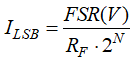
Equation 12 yields 305pA per bit resolution for the 200kΩ feedback resistor, and 30.5nA resolution for a 2kΩ resistor. Table 3-1 shows the current range, output voltage range, and the desired TIA bandwidth and resolution for this design.
| Current Range | Gain | Vout (Max) | Resolution |
|---|---|---|---|
| 0-20µA | 200kV/A | 4 V @ 20µA | 0.305 nA/bit |
| 20µA - 2mA | 2kV/A | 4 V @ 2mA | 30.5 nA/bit |
4 Stability of the Transimpedance Amplifier
The circuit designer must verify the minimum necessary op-amp gain-bandwidth to guarantee stability and select the appropriate feedback compensation capacitor for each TIA gain. Therefore, it is essential to consider factors that affect TIA circuit stability carefully: the junction capacitance of the photodiode (CJ), the TIA gain, the desired closed-loop TIA bandwidth, and the unity gain-bandwidth product of the op-amp (fGBW).
The circuit diagram on Figure 4-1 shows the photodiode reverse junction capacitance (CJ) and the differential and common mode input capacitance of the of-amp (CDIFF, CCM1,2).
 Figure 4-1 Photodiode Transimpedance Amplifier and Total Parasitic Capacitance
Figure 4-1 shows the total capacitance at the input of the amplifier. This capacitance is the parallel combination of the photodiode capacitance, and the amplifier differential and common-mode input capacitance. Since the non-inverting terminal connects to an AC ground, the CCM1 common-mode capacitor does not contribute to the total input capacitance:
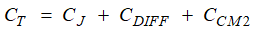
The OPA3S328 offers a differential capacitance of approximately, CDIFF = 3.8pF, and the common-mode capacitance, CCM2 = 1.2pF. Accounting for the photodiode junction capacitance, the total capacitance at the input of the amplifier CT is approximately 105pF.
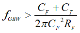
The TIA circuit stability is related to the amplifier’s loop gain and the loop gain phase response. The loop-gain is the product of the op amp’s open-loop gain (AOL) and the circuit feedback factor (β), where the circuit’s loop-gain is (AOL * β). Phase margin is a stability metric which compares the phase of the loop-gain (AOL * β) of an amplifier to 180 degrees at the point where loop gain equals 0-dB and marks the frequency where AOL and the 1/ β bode plots intersect.
One method to determine the stability of the circuit is called the rate of closure analysis. In this method, we consider the rate of closure of AOL and 1/ β at frequency fC, the point in frequency where the magnitude plots intersect. This method's rule is that the difference in the slope of the AOL magnitude and the slope of the 1/ β magnitude plots must be ideally close to 20-dB or less to ensure optimal stability.
Figure 4-2 shows the bode plots of the AOL for a high bandwidth amplifier and the AOL for a lower bandwidth amplifier, along with the 1/β curve of a typical TIA.
 Figure 4-2 AOL and 1/β plot for Transimpedance Op Amp Circuit
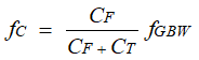
The 1/β magnitude plot, also referred to as the non-inverting gain or noise gain, presents a zero (fZ) and a pole (fP) on its frequency response. Above the zero frequency (fZ), the 1/β plot increases a rate of +20dB per decade. At frequencies above the pole (fP), the 1/β curve remains flat. The frequency fC is the frequency point where the AOL and 1/β magnitude plots intersect, and this frequency is a function of the unity gain-bandwidth product of the amplifier fGBW, the feedback capacitor, CF, and the total input capacitance of the amplifier, CT:
By analyzing the rate of closure (ROC) of AOL and 1/β when the curves intersect, we can determine the stability of the circuit. The rule of thumb for this method is that the rate of closure must ideally be close to 20-dB/decade for optimal stability. Therefore, to maintain stability, the AOL curve must intersect the 1/β curve when the 1/β curve is flat. If the AOL curve intersects the 1/β curve when the 1/β curve is rising, as shown by the lower bandwidth op amp AOL curve in Figure 4-2, the rate of closure is 40-dB and the circuit will likely be unstable, leading to unwanted oscillations, long settling time and intermittent or unfavorable circuit behaviors.
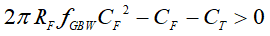
Equation 5 provides the necessary condition for the transimpedance amplifier stability:

Substituting the equations for fC and fP into the inequality provided on Equation 5 yields to Equation 6
The inequality can be re-arranged as a quadratic equation in terms of the feedback capacitor, CF, as shown in Equation 12:
Solving for CF using the general quadratic formula and obtaining the only real positive solution yields the result shown in Equation 8:
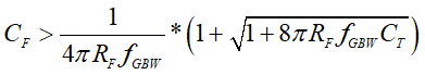
Equation 8 determines the minimum compensation capacitor to guarantee stability for the TIA design. Table 4-1 shows the minimum calculated compensation capacitors CF1 and CF2 to ensure stability for each TIA gain for the unity gain-bandwidth of the OPA3S328. The dominant pole frequency fP is a function of the feedback resistor and feedback capacitor for each TIA gain.
| fGBW Amplifier Unity Gain Bandwidth |
TIA Gain | CT TIA Total Input Capacitance |
RF TIA Feedback Resistor |
CF Min Feedback Capacitor for stability |
fP Dominant Pole frequency |
|---|---|---|---|---|---|
| 40 MHz | 200 kV/A | 105 pF | 200 kΩ | >1.5pF | 530kHz |
| 40 MHz | 2 kV/A | 105 pF | 2 kΩ | >16pF | 4.97MHz |
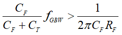
A different approach to ensure stability while meeting a TIA gain and bandwidth requirement, is to use the inequality provided in Equation 6, and solve for the amplifier's minimum unity gain-bandwidth (fGBW). Equation 9 provides the amplifier's minimum fGBW as a function of the feedback resistor RF, the feedback capacitor CF, and the total input capacitance of the amplifier CT:
Equation 9 determines the amplifier's minimum required unity gain-bandwidth to guarantee stability for a TIA design. Therefore, higher bandwidth amplifiers support higher gain and bandwidth TIA circuits, and tolerate higher photodiode capacitance while remaining stable.
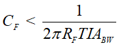
On this programmable gain TIA example, the desired closed-loop bandwidth TIABW is 500kHz. Therefore, Equation 10 provides the maximum compensation capacitance CF while meeting the closed loop TIA bandwidth requirement:
Equation 10 shows the calculated compensation capacitors CF1 and CF2 for each gain to meet the TIA closed-loop bandwidth requirement and the required amplifier's minimum unity gain-bandwidth to ensure stability:
| TIA Gain | TIABW Desired TIA Bandwidth |
CT TIA Total Input Capacitance |
RF TIA Feedback Resistor |
CF Feedback Capacitor for TIABW |
fGBW Min Amplifier Unity Gain BW |
|---|---|---|---|---|---|
|
200 kV/A |
500 kHz |
105 pF |
200 kΩ |
1.6pF |
> 33.8MHz |
|
2 kV/A |
500 kHz |
105 pF |
2 kΩ |
159pF |
> 834 kHz |
The OPA3S328 offers a unity gain bandwidth of 40 MHz, and therefore, can support the desired TIA gain and bandwidth requirements for the design. Select standard values for the compensation capacitor, CF1 = 1.6pF for TIA gain of 200kV/A and CF2 of 150pF for TIA gain of 2kV/A.
Verify the stability for each gain using TINA SPICE simulations. Figure 4-3 shows the TINA-TI circuit schematic used to analyze stability. Use a large inductor (L1) to break the loop at the input of the amplifier. The test voltage source is AC coupled through the large capacitor (C1). Since the feedback loop is open at the op-amp input, add the op-amp input capacitance, CDIFF and CCM2 into the schematic next to inductor L1. Use the simulator post-processor to generate the open-loop gain (AOL) and noise gain (1/β) curves for each gain setting. Figure 4-4 shows the stability analysis simulation results for RF1 = 200kΩ, CF1 = 1.6pF and Figure 4-5 for RF2 = 2kΩ, CF2=150pF.
 Figure 4-3 TINA-TI Circuit Schematic to Analyze Programmable Gain TIA Stability
 Figure 4-4 Stability Analysis for RF1 = 200kΩ
 Figure 4-5 Stability Analysis for RF2 = 2kΩ
5 Integrated Switch Characteristics
The OPA3S328 incorporates two sets of low leakage, low capacitance and low on-resistance switches useful for different circuit configurations, including programmable gain transimpedance applications. The QFN package version of the OPA3S328 device features switch 1 in a 1:2 matrix configuration, one input (INSA) with two outputs (OUTSA1, 2) and switch 2, in a 1:3 matrix configuration, one input (INSB) with three outputs (OUTSB1, 2, 3). On this circuit example, switch 1 is used to build the programmable gain TIA.
Table 5-1 shows key switch parameters based on the OPA3S328 data sheet specifications:
| Parameter | Test Condition | Min | TYP | Max | Unit |
|---|---|---|---|---|---|
| CIN Switch input capacitance | Switch open, INSA/B = 2.5 V | 2.3 | pF | ||
| COUT Switch output capacitance | Switch open, OUTSA/B/1/2/3 = 2.5 V | 0.7 | pF | ||
| CINOUT Switch total capacitance | Switch closed, INSA/B = OUTSA/B/1/2/3 = 2.5 V | 6 | pF | ||
| RON Switch on resistance | Switch closed, V+ = 5 V, INSA/B = 2.5 V | 90 | 125 | Ω |
CIN and COUT represent the open switch parasitic switch capacitance, while CINOUT represents the total switch capacitance while the switch is closed. RON is the switch series resistance when the switch is closed. Figure 5-1 shows a simplified model based on the switch data sheet parameters used in the TINA simulations using the switch input and output capacitances and the switch on resistance:
 Figure 5-1 OPA3S328 Simplified Switch Model
When designing the switch gain transimpedance amplifier, the designer needs to consider the non-ideal characteristics of the switches. The bandwidth and stability of the transimpedance will be affected by the capacitances and resistances of the switch. Furthermore, the on-resistance RON of the switch can be a source of error on the gain of the transimpedance amplifier. The following sections discuss errors due to the switch non-ideal behavior and proposes circuits to overcome these errors.
