SBOA521 June 2021 OPA3S328
6 Frequency Response Simulations
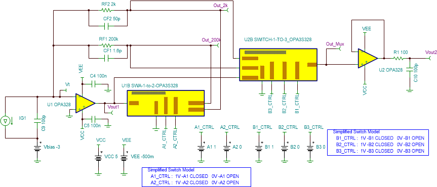
Figure 6-1 shows the TINA-TI Schematic of the complete programmable gain transimpedance amplifer, including the buffer amplifier with Kelvin sense connections. Sub-circuits SWA and SWB model the switches capacitance and on-resistance.
 Figure 6-1 TINA-TI Schematic of Complete
Programmable Gain TIA
Figure 6-1 TINA-TI Schematic of Complete
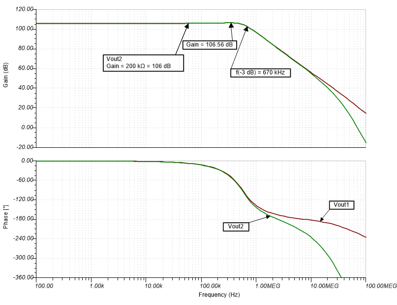
Programmable Gain TIAFigure 6-1 displays the simulation result for the TIA closed-loop frequency response with a gain of 200-kV/A, showing a corner frequency of 670kHz, exceeding the frequency response requirement.
 Figure 6-2 Frequency Response Simulation Result for RF1 = 200kΩ,
CF1=1.6pF
Figure 6-2 Frequency Response Simulation Result for RF1 = 200kΩ,
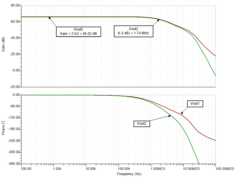
CF1=1.6pFFigure 6-1 displays the simulation result for the TIA closed-loop frequency response with a gain of 200-kV/A, showing a corner frequency of 1.6MHz.
 Figure 6-3 Frequency Response Simulation Result for RF2 = 2kΩ,
CF2=50pF
Figure 6-3 Frequency Response Simulation Result for RF2 = 2kΩ,
CF2=50pFBoth transimpedance amplifier gains showcase an AC response meeting the frequency response requirement with robust stability with very subtle peaking at the TIA output (less than <0.5dB, consistent with the ~55-degree phase margin of the circuit.