SBOA521 June 2021 OPA3S328
3 The Programmable Gain Transimpedance Amplifier
One method to implement a programmable gain TIA is to use a TIA stage cascaded by a second Programmable Gain Amplifier (PGA) stage, as shown in Figure 3-1. The TIA gain is set according to the maximum current range from the photodiode. Then, the user adjusts the PGA according to the photodiode current conditions; in other words, the user sets the gain to 1V/V under high photodiode current conditions, or selects a higher gain under low-light current conditions producing an optimal output voltage range. The total output noise of the cascaded TIA and PGA circuit is the TIA's output noise multiplied by the PGA gain plus the noise contribution of the PGA gain stage.
 Figure 3-1 TIA Stage Cascaded with PGA Stage
A better approach is to use a single-stage transimpedance amplifier with programmable gain, adjusting the TIA feedback resistor according to the photodiode current condition. This approach provides a significant advantage from the noise performance perspective since the signal is gained on a single transimpedance stage, resulting in lower total output noise. Figure 3-2 shows a programmable gain TIA using the OPA3S328. The integrated 1:2 analog switch selects the different transimpedance feedback resistor. Each transimpedance gain resistor RF1 and RF2 requires its feedback capacitor, CF1, and CF2, to stabilize the amplifier and compensate for the photodiode junction capacitance.
 Figure 3-2 Switched Gain Transimpedance Amplifier
The TIA gain needs to be selected to align with the voltage range of the data acquisition system. In this example, the OPA3S328 drives a 16-Bit ADC with a full-scale range of 4V. Select the feedback resistor values RF1 and RF2 by dividing the full-scale voltage range by the photodiode current range for each gain. In this design, let RF1 = 200-kΩ and RF2 = 2-kΩ for a 0-20µA and 20µA - 2mA photodiode current range respectively.
Equation 12 provides the current measurement resolution least significant bit size (ILSB), for each gain, where FSR is the full-scale range of the ADC in volts, and N represents the bit resolution of the ADC:
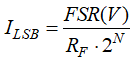
Equation 12 yields 305pA per bit resolution for the 200kΩ feedback resistor, and 30.5nA resolution for a 2kΩ resistor. Table 3-1 shows the current range, output voltage range, and the desired TIA bandwidth and resolution for this design.
| Current Range | Gain | Vout (Max) | Resolution |
|---|---|---|---|
| 0-20µA | 200kV/A | 4 V @ 20µA | 0.305 nA/bit |
| 20µA - 2mA | 2kV/A | 4 V @ 2mA | 30.5 nA/bit |