SBOA521 June 2021 OPA3S328
5.1 TIA Stability and Switch Capacitance
Although the OPA3S328 integrated switches offer relatively low parasitic capacitance and low on resistance, the designer needs to verify the effect of the switches to ensure the stability of the circuit. Using the same open-loop simulation circuit of Figure 4-2, we add the simplified switch model and plot the loop gain, AOL, and 1/Beta to analyze stability.
Figure 5-2 show the TINA-TI circuit schematic used to analyze stability incorporating the simplified switch model for each gain. Perform an AC transfer characteristic simulation and use the post-processor to generate the open-loop gain (AOL) and noise gain (1/β) curves for each gain setting. Figure 5-2 shows the stability analysis simulation results for RF1 = 200kΩ, CF1=1.6pF including the integrated switch capacitance.
 Figure 5-2 TINA-TI Schematic for Stability Analysis Including Switches
 Figure 5-3 Stability Analysis for
RF1 = 200kΩ, CF1 = 1.6pF with Switch
Figure 5-3 Stability Analysis for
RF1 = 200kΩ, CF1 = 1.6pF with SwitchAfter adding the switch parasitic components, the stability analysis for RF1 = 200kΩ and CF1 = 1.6pF shows the AOL and 1/β curves intersect with a rate of closure of -20 dB/decade. The phase margin remains higher than 45-degrees, guaranteeing robust circuit stability for this gain.
Figure 5-4 displays the results for RF2= 2kΩ and CF2=150pF.
 Figure 5-4 Stability Analysis for RF2 = 2kΩ, CF2 = 150pF with
Switch
Figure 5-4 Stability Analysis for RF2 = 2kΩ, CF2 = 150pF with
SwitchThe RON switch resistance interacts with the series combination of the feedback capacitor CF2 and the total capacitance at the input of the amplifier CT, generating an additional zero fZ2 on the 1/β curve. Equation 11 defines the second zero frequency on the 1/β curve:
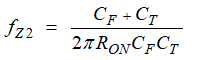
fZ2 degrades the phase margin to ~36-degrees. The previous calculation in Table 4-1 and Table 4-2 shows that the permissible feedback capacitor range for CF2 is between 16pF and 159pF. To improve phase margin, reduce the feedback capacitor CF2 to 50pF, moving the second zero fZ2, to a higher frequency than the amplifier's unity gain-bandwidth of 40-MHz, where the effect fZ2 on the circuit stability is negligible. Figure 5-5 displays the stability analysis results for the revised circuit with RF2= 2kΩ and CF2=50pF. The phase margin improves to 57-degrees, guaranteeing robust circuit stability.
 Figure 5-5 Stability Analysis for Revised Circuit with RF2 = 2kΩ,
CF2 = 50pF
Figure 5-5 Stability Analysis for Revised Circuit with RF2 = 2kΩ,
CF2 = 50pF