SBOA521 June 2021 OPA3S328
2 The Transimpedance Amplifier and Photodiode Sensor
A transimpedance amplifier consists of an op amp and a feedback resistor. The photosensor current to be amplified is applied to the inverting input, causing the output voltage of the amplifier to change, as shown in Figure 2-1:
 Figure 2-1 Photodiode Transimpedance Amplifier
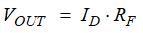
The feedback resistor (RF) across the op amp converts the photodiode current (ID) to a voltage (VOUT) using Ohm’s law, as shown in Equation 12.
The feedback resistor (RF) determines the gain of the transimpedance op-amp. For the transimpedance current to voltage conversion to be accurate, the amplifier’s input bias current and input offset voltage must be small. The OPA3S328 offers low offset voltage, 25µV (max) and low input bias current, 0.2 pA. The photodiode parasitic junction capacitance plays a significant role in the stability and bandwidth of the TIA circuit, as we will discuss in detail in the following sections. The feedback capacitor (CF) is required to compensate the circuit for stability.
This example shows a large area near-infrared (NIR) wavelength Indium Gallium Arsenide (InGaAs) photodiode for the design. In this specific application, the photodiode operates on the photoconductive mode, where exposure to light causes a reverse current through the detector. A reverse bias is applied to the photosensor to reduce the junction capacitance. The reverse bias voltage (VR) dramatically improves the speed of response and linearity of the photodiode. The reverse bias increases the depletion region width and consequently decreases the junction capacitance. The dark current of this photosensor is about 50nA in this mode of operation. Table 2-1 shows the photodiode parameters.
| Parameter | Symbol | Value | Unit |
|---|---|---|---|
| Reverse Voltage | VR | -3 | V |
| Junction Capacitance (VR=-3V) | CJ | 100 | pF |
| Reverse Current Range | ID | 0-2000 | µA |
| Dark Current | Idark | 50 | nA |
There are different ways to bias the photodiode in the TIA circuit. A common method used on unipolar supply applications is to bias the op-amp non-inverting input (+IN) with a positive dc voltage. The positive voltage at the non-inverting input will reverse bias the photodiode while allowing the amplifier output to reach true zero when the photodiode is unexposed to light and respond without the added delay that results from coming out of the negative rail. Figure 2-2 shows a typical way to reverse bias the photodiode, when the reverse voltage required is relatively small.
 Figure 2-2 Unipolar-Supply Transimpedance Amplifier
However, in this example, the diode requires a relatively large reverse bias voltage of -3V when compared to the 5.5V maximum voltage supply range of the OPA3S328. A different method to reverse bias the diode is to apply the negative bias voltage (VR = -3V) directly to the photodiode's anode. This configuration is shown in Figure 2-3.
 Figure 2-3 Bipolar-Supply Transimpedance Amplifier
The non-inverting OPA3S328 terminal connects to ground and the amplifier is powered with bipolar asymmetrical supplies, Vcc = +5 V and Vee = -0.5 V, allowing the dc voltage output to reach true zero when the diode is not exposed to light. In addition, this circuit makes better use of the OPA3S328 output voltage range, allowing a large diode reverse bias voltage without impacting the voltage range of the output signal.