SBOA521 June 2021 OPA3S328
5.3 TIA Gain Error due to Switch On-Resistance
The switch RON resistance will produce DC gain errors and distortion on the transimpedance amplifier. The percent gain error is dependent on the TIA feedback resistor value; and the gain errors are relatively large at the lower feedback resistor values. For example, with the RF1 = 200kΩ resistor, the maximum switch RON resistance of 125Ω will contribute about 0.063% gain error. In the case of the lower RF2=2kΩ resistor, the gain error due to the switch RON resistance is much more significant, about 6.25% gain error. In addition, the switch on resistance changes with temperature producing TIA gain drift errors.
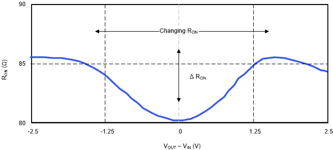
Furthermore, the RON switch resistance of each selectable gain varies over the TIA output voltage. Figure 5-7 shows the change of RON resistance vs the voltage difference across the switch.
 Figure 5-7 RON Resistance Vs Voltage
This ΔRON change in switch resistance introduces signal-dependent distortion and gain error linearity based on the switch impedance.
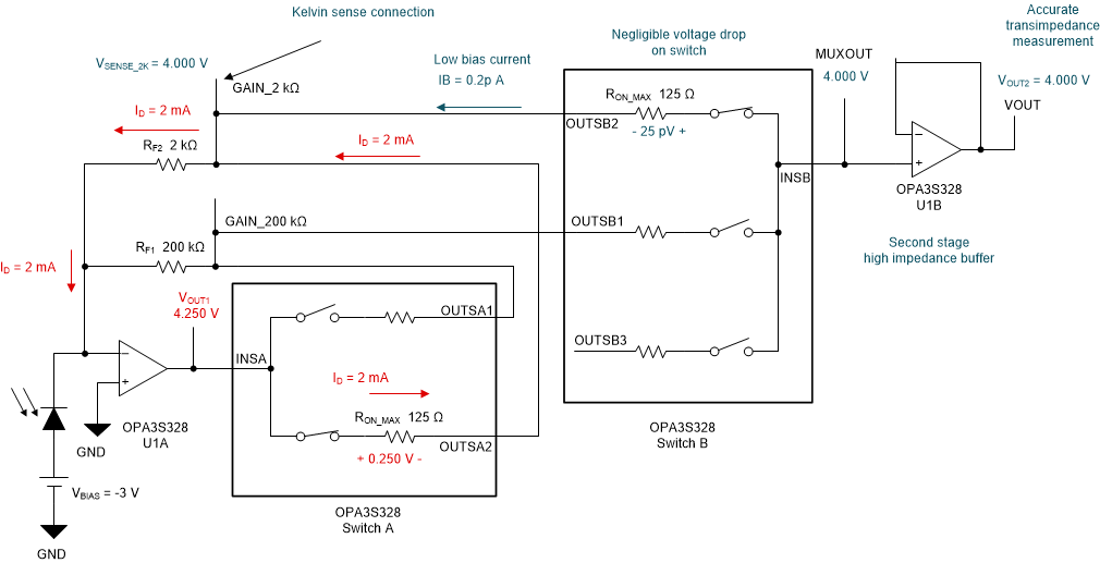
One way to address this issue is to build a multiplexer using the second integrated switch of the OPA3S328. The multiplexer input senses the TIA output connection for the selected gain right at the RF feedback resistor terminal. The second amplifier stage is configured in a high impedance non-inverting configuration, buffering the multiplexer and providing an accurate Kelvin sense connection of the TIA output for each gain. Since the input bias current of the op-amp is minimal, < 10pA, the voltage drop across the switch RON resistance is negligible. Figure 5-8 shows the OPA3S328 circuit using the 3:1 switch B to build the Kelvin sense connection multiplexer, buffered with a second-stage amplifier. The voltage drop across the RON resistance of switch SB2 is negligible.
 Figure 5-8 Switch Kelvin Sense Connections and High Impedance Buffer
The Kelvin sense connections eliminate the gain error, gain error drift and gain non-linearity due to the switch RON resistances though the high impedance second-stage amplifier. The second-stage could also be configured in a non-inverting gain configuration, adding the flexibility for even higher gains while maintaining the circuit bandwidth.