SBOA597 November 2024 OPA928
4 Calibration Using a Coulombmeter for Application Circuits
Previous sections described the limits and precautions of the measurement. To realize a full design, the coulombmeter circuit deploys:
- A polypropylene capacitor for an integrator that resistance was measured as tens of PΩ at the room temperature.
- Double layer metal shielding to prevent coupling electric field to the high-impedance node.
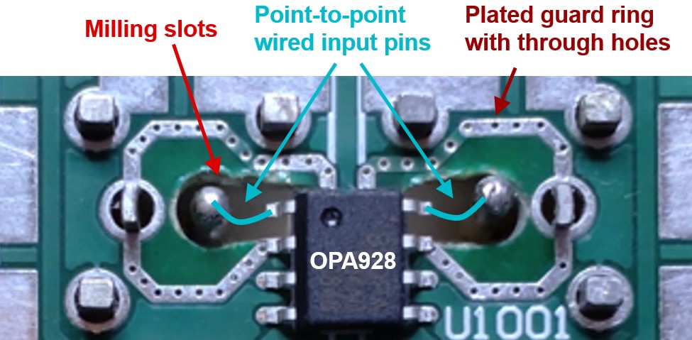
- Point-to-point wiring for high-impedance nodes.
- Cleanliness.
Figure 4-1 shows an example of a PCB that can allow for both standard surface-mount devices, along with point-to-point wiring. The layout specifically around the input high-impedance nodes of the circuit has milled slots with point-to-point wiring; see below.
 Figure 4-1 OPA928 Calibration Board
Layout for the High-Impedance Node