SBOA606 October 2024 OPT4001-Q1
2 Assembly
With the bottom facing assembly, the PicoStar™ package requires a cutout in the flex PCB (FPCB) to allow light to reach the sensing area. Increasing the cutout size can maximize the field of view of the sensor resulting in the best optical performance. The maximum cutout size can be limited by the manufacturing capability of the FPCB fabrication and assembly shop. Figure 2-1 illustrates two options for PCB cut out shape (plus shape and circular shape). The clearance required between the PCB pads and the cutout can typically be very small and can require consultation with the FPCB vendor.
 Figure 2-1 Flex PCB Cutout Recommendations
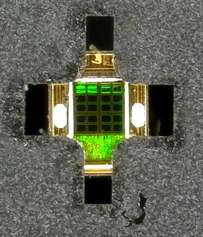
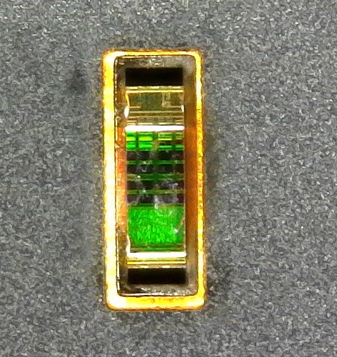
With the 4-pin design on OPT4001YMN, the diagonal distance between the pads is >800µm, which enables a cutout with very large field of view (>50°) with a simple circular cutout. Using a plus-shaped cutout maximizes the field of view even further in the directions where the pads do not restrict enabling best optical performance. A rectangular cutout can enable the largest field-of-view in one direction similar to the plus cutout, but can restrict the field-of-view somewhat in the opposing direction. Examples of PCB layout and cutout shapes for the plus and rectangular cases are shown in the following images.
 Figure 2-2 Layout Example With a Plus Shaped Cut Out
 Figure 2-4 Image of FPCB With OPT4001YMN-Q1 Mounted, Receiving Light Through the Cutout with a Plus Shape
 Figure 2-3 Layout Example With a Rectangular Shaped Cut Out
 Figure 2-5 Image of FPCB With OPT4001YMN-Q1 Mounted, Receiving Light Through the Cutout with a Rectangular Shape