SBOS223H December 2001 – October 2024 OPA690
PRODUCTION DATA
- 1
- 1 Features
- 2 Applications
- 3 Description
- 4 Device Comparison Table
- 5 Pin Configuration and Functions
-
6 Specifications
- 6.1 Absolute Maximum Ratings
- 6.2 ESD Ratings
- 6.3 Recommended Operating Conditions
- 6.4 Thermal Information
- 6.5 Electrical Characteristics OPA690IDBV, VS = ±5 V
- 6.6 Electrical Characteristics OPA690IDBV, VS = 5 V
- 6.7 Electrical Characteristics OPA690ID, VS = ±5 V
- 6.8 Electrical Characteristics OPA690ID, VS = 5 V
- 6.9 Typical Characteristics: OPA690IDBV, VS = ±5V
- 6.10 Typical Characteristics: OPA690IDBV, VS = 5V
- 6.11 Typical Characteristics: OPA690ID, VS = ±5V
- 6.12 Typical Characteristics: OPA690ID, VS = 5V
- 7 Detailed Description
- 8 Application and Implementation
- 9 Device and Documentation Support
- 10Revision History
- 11Mechanical, Packaging, and Orderable Information
8.1.2 Inverting Amplifier Operation
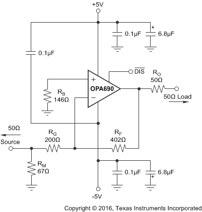
The OPA690 is a general-purpose, wideband voltage-feedback op amp; therefore, all of the familiar op amp application circuits are available to the designer. Inverting operation is one of the more common requirements and offers several performance benefits. Figure 8-1 shows a typical inverting configuration where the I/O impedances and signal gain from Figure 7-1 are retained in an inverting circuit configuration.
 Figure 8-1 Gain of –2 V/V Example
Circuit
Figure 8-1 Gain of –2 V/V Example
CircuitIn the inverting configuration, be aware of three key design considerations. The first consideration is that the gain resistor (RG) becomes part of the signal channel input impedance. If input impedance matching is desired (which is beneficial whenever the signal is coupled through a cable, twisted-pair, long PCB trace, or other transmission line conductor), RG can be set equal to the required termination value and RF adjusted to give the desired gain. This configuration is the simplest approach and results in optimized bandwidth and noise performance. However, at low inverting gains, the resultant feedback resistor value can present a significant load to the amplifier output. For an inverting gain of 2 V/V, setting RG to 50 Ω for input matching eliminates the requirement for RM but requires a 100-Ω feedback resistor. This configuration has an interesting advantage: the noise gain becomes equal to 2 for a 50-Ω source impedance—the same as the noninverting circuits considered in the previous section. The amplifier output, however, now sees the 100-Ω feedback resistor in parallel with the external load. In general, limit the feedback resistor to the 200-Ω to 1.5-kΩ range. In this case, increase both the RF and RG values, as shown in Figure 8-1, and then achieve the input matching impedance with a third resistor (RM) to ground. The total input impedance becomes the parallel combination of RG and RM.
The second major consideration, touched on in the previous paragraph, is that the signal source impedance becomes part of the noise gain equation and influences the bandwidth. For the example in Figure 8-1, the RM value combines in parallel with the external 50-Ω source impedance, yielding an effective driving impedance of 50 Ω || 67 Ω = 28.6 Ω. This impedance is added in series with RG for calculating the noise gain (NG). The resultant NG is 2.8 for Figure 8-1, as opposed to only 2 if RM can be eliminated as discussed previously. Therefore, the bandwidth is slightly less for the circuit of Figure 8-1 than for the gain of 2 circuit of Figure 7-1.
The third important consideration in inverting amplifier design is setting the bias current cancellation resistor on the noninverting input (RB). If this resistor is set equal to the total dc resistance looking out of the inverting node, the output dc error, due to the input bias currents, is reduced to (Input Offset Current) × RF. If the 50-Ω source impedance is dc-coupled in Figure 8-1, the total resistance to ground on the inverting input is 228 Ω. Combining this in parallel with the feedback resistor gives the RB = 146 Ω used in this example. To reduce the additional high-frequency noise introduced by this resistor, the resistor is sometimes bypassed with a capacitor. As long as RB < 350 Ω, the capacitor is not required because the total noise contribution of all other terms is less than that of the op-amp input noise voltage. As a minimum, the OPA690 requires an RB value of 50 Ω to damp out parasitic-induced peaking that is a direct short to ground on the noninverting input, and runs the risk of a very high-frequency instability in the input stage.