SBOS293I December 2003 – October 2024 OPA695
PRODUCTION DATA
- 1
- 1 Features
- 2 Applications
- 3 Description
- 4 Pin Configuration and Functions
-
5 Specifications
- 5.1 Absolute Maximum Ratings
- 5.2 ESD Ratings
- 5.3 Recommended Operating Conditions
- 5.4 Thermal Information
- 5.5 Electrical Characteristics VS = ±5 V, OPA695ID, OPA695IDBV
- 5.6 Electrical Characteristics VS = 5 V, OPA695ID, OPA695IDBV
- 5.7 Electrical Characteristics VS = ±5 V, OPA695IDGK
- 5.8 Electrical Characteristics VS = 5 V, OPA695IDGK
- 5.9 Typical Characteristics: VS = ±5 V, OPA695IDBV, OPA695ID
- 5.10 Typical Characteristics: VS = 5 V, OPA695IDBV, OPA695ID
- 5.11 Typical Characteristics: VS = ±5 V, OPA695IDGK
- 5.12 Typical Characteristics: VS = 5 V, OPA695IDGK
- 6 Detailed Description
- 7 Application and Implementation
- 8 Device and Documentation Support
- 9 Revision History
- 10Mechanical, Packaging, and Orderable Information
7.1.4 Differential I/O Applications
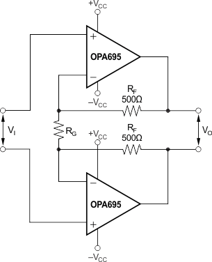
The OPA695 offers very low 3rd-order distortion terms with a dominant 2nd-order distortion for the single amplifier operation. For the lowest distortion, particularly where differential outputs are needed, operating two OPA695 devices in a differential I/O design suppresses these even-order terms, delivering extremely low harmonic distortion through high frequencies and powers. Differential outputs are often preferred for high-performance ADCs, twisted-pair driving, and mixer interfaces. Two basic approaches to differential I/Os are the noninverting or inverting configurations. Because the output is differential, the signal polarity is somewhat meaningless; the noninverting and inverting terminology applies here to where the input is brought into the two OPA695s. Each approach has advantages and disadvantages. Figure 7-8 shows a basic starting point for noninverting differential I/O applications.
 Figure 7-8 Noninverting Input Differential I/O Amplifier
This approach allows for a source termination impedance independent of the signal gain. For instance, simple differential filters can be included in the signal path directly to the noninverting inputs without interacting with the gain setting. The differential signal gain for the circuit of Figure 7-8 is:
Because the OPA695 is a current-feedback amplifier, bandwidth is principally controlled with the feedback resistor value: Figure 7-8 shows a typical value of 500 Ω. However, the differential gain can be adjusted with considerable freedom using just the RG resistor. RG can be a reactive network providing an isolated shaping to the differential frequency response. AC-coupled applications often include a blocking capacitor in series with RG. This blocking capacitor reduces the gain to +1 V/V at low frequency, rising to the AD expression shown previously at higher frequencies.
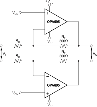
Figure 7-9 shows a differential I/O stage configured as an inverting amplifier. In this case, the gain resistors (RG) become part of the input resistance for the source. This configuration provides a better noise performance than the noninverting configuration, but limits the flexibility in setting the input impedance separately from the gain.
 Figure 7-9 Inverting Input Differential I/O Amplifier
The two noninverting inputs provide an easy common-mode control input, particularly if the source is ac-coupled through either blocking caps or a transformer. In either case, the common-mode input voltages on the two noninverting inputs again have a gain of +1 V/V to the output pins, giving easy common-mode control for single-supply operation. In this configuration, the OPA695 constrains the feedback to the 500-Ω region for best frequency response. With RF fixed, the input resistors can be adjusted to the desired gain, but also change the input impedance. The high-frequency common-mode gain for this circuit from input to output is the same as for the signal gain. Again, if the source includes an undesired common-mode signal, the signal can be rejected at the input using blocking caps (for low-frequency and dc common-mode) or a transformer coupling. The differential signal gain in the circuit of Figure 7-9 is:
Using this configuration suppresses the 2nd-harmonics, leaving only 3rd-harmonic terms as the limit to output SFDR. The higher slew rate of the inverting configuration also extends the full-power bandwidth and the range of low intermodulation distortion over the performance bandwidth available from the circuit of Figure 7-8.