SBOS293I December 2003 – October 2024 OPA695
PRODUCTION DATA
- 1
- 1 Features
- 2 Applications
- 3 Description
- 4 Pin Configuration and Functions
-
5 Specifications
- 5.1 Absolute Maximum Ratings
- 5.2 ESD Ratings
- 5.3 Recommended Operating Conditions
- 5.4 Thermal Information
- 5.5 Electrical Characteristics VS = ±5 V, OPA695ID, OPA695IDBV
- 5.6 Electrical Characteristics VS = 5 V, OPA695ID, OPA695IDBV
- 5.7 Electrical Characteristics VS = ±5 V, OPA695IDGK
- 5.8 Electrical Characteristics VS = 5 V, OPA695IDGK
- 5.9 Typical Characteristics: VS = ±5 V, OPA695IDBV, OPA695ID
- 5.10 Typical Characteristics: VS = 5 V, OPA695IDBV, OPA695ID
- 5.11 Typical Characteristics: VS = ±5 V, OPA695IDGK
- 5.12 Typical Characteristics: VS = 5 V, OPA695IDGK
- 6 Detailed Description
- 7 Application and Implementation
- 8 Device and Documentation Support
- 9 Revision History
- 10Mechanical, Packaging, and Orderable Information
7.1.2 LO Buffer Amplifier
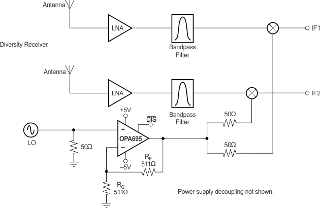
The OPA695 can also be used to buffer the local oscillator (LO) from the mixer. Operating at a voltage gain of +2 V/V, the OPA695 provides excellent load isolation for the LO, with a net gain of 0 dB to the mixer. Applications through a 1.4-GHz LO can be considered, but best operation is for an LO < 1.0 GHz at a gain of +2 V/V. Gain can also be provided by the OPA695 to drive higher power levels into the mixer. Figure 7-5 shows one option for the OPA695 as an LO buffer. The OPA695 can drive multiple output loads; therefore, two identical LO signals can be delivered to the mixers in a diversity receiver by tapping the output off through two series 50-Ω output resistors. This circuit is set up for a voltage gain of +2 V/V to the output pin for a gain of +1 V/V (0 dB) to the mixers, but can be easily adjusted to deliver higher gains.
 Figure 7-5 Dual Output LO Buffer