SBOS397I August   2007  – June 2024 TMP102

PRODUCTION DATA  

  1.   1
  2. Features
  3. Applications
  4. Description
  5. Pin Configuration and Functions
  6. Specifications
    1. 5.1 Absolute Maximum Ratings
    2. 5.2 ESD Ratings
    3. 5.3 Recommended Operating Conditions
    4. 5.4 Thermal Information
    5. 5.5 Electrical Characteristics
    6. 5.6 Timing Requirements
    7. 5.7 Typical Characteristics
  7. Detailed Description
    1. 6.1 Overview
    2. 6.2 Functional Block Diagram
    3. 6.3 Feature Description
      1. 6.3.1  Digital Temperature Output
      2. 6.3.2  Serial Interface
      3. 6.3.3  Bus Overview
      4. 6.3.4  Serial Bus Address
      5. 6.3.5  Writing and Reading Operation
      6. 6.3.6  Target Mode Operations
        1. 6.3.6.1 Target Receiver Mode
        2. 6.3.6.2 Target Transmitter Mode
      7. 6.3.7  SMBus Alert Function
      8. 6.3.8  General Call
      9. 6.3.9  High-Speed (HS) Mode
      10. 6.3.10 Timeout Function
      11. 6.3.11 Timing Diagrams
    4. 6.4 Device Functional Modes
      1. 6.4.1 Continuous-Conversion Mode
      2. 6.4.2 Extended Mode (EM)
      3. 6.4.3 Shutdown Mode (SD)
      4. 6.4.4 One-Shot/Conversion Ready (OS)
      5. 6.4.5 Thermostat Mode (TM)
        1. 6.4.5.1 Comparator Mode (TM = 0)
        2. 6.4.5.2 Interrupt Mode (TM = 1)
    5. 6.5 Programming
      1. 6.5.1 Pointer Register
      2. 6.5.2 Temperature Register
      3. 6.5.3 Configuration Register
        1. 6.5.3.1 Shutdown Mode (SD)
        2. 6.5.3.2 Thermostat Mode (TM)
        3. 6.5.3.3 Polarity (POL)
        4. 6.5.3.4 Fault Queue (F1/F0)
        5. 6.5.3.5 Converter Resolution (R1/R0)
        6. 6.5.3.6 One-Shot (OS)
        7. 6.5.3.7 EM Bit
        8. 6.5.3.8 Alert (AL Bit)
        9. 6.5.3.9 Conversion Rate (CR)
      4. 6.5.4 High- and Low-Limit Registers
  8. Application and Implementation
    1. 7.1 Application Information
    2. 7.2 Typical Application
      1. 7.2.1 Design Requirements
      2. 7.2.2 Detailed Design Procedure
      3. 7.2.3 Application Curve
    3. 7.3 Power Supply Recommendations
    4. 7.4 Layout
      1. 7.4.1 Layout Guidelines
      2. 7.4.2 Layout Example
  9. Device and Documentation Support
    1. 8.1 Documentation Support
      1. 8.1.1 Related Documentation
    2. 8.2 Receiving Notification of Documentation Updates
    3. 8.3 Support Resources
    4. 8.4 Trademarks
    5. 8.5 Electrostatic Discharge Caution
    6. 8.6 Glossary
  10. Revision History
  11. 10Mechanical, Packaging, and Orderable Information

Pin Configuration and Functions

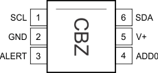
TMP102 DRL Package6-Pin SOT563Top ViewFigure 4-1 DRL Package6-Pin SOT563Top View
Table 4-1 Pin Functions
PINTYPE(1)DESCRIPTION
NO.NAME
1SCLISerial clock
2GNDGround
3ALERTOOvertemperature alert. Open-drain output; requires a pullup resistor.
4ADD0IAddress select. Connect to GND or V+
5V+ISupply voltage, 1.4 V to 3.6 V
6SDAI/OSerial data. Open-drain output; requires a pullup resistor.
I = Input, O = Output, I/O = Input or Output