SBOS516H September   2010  – June 2024 OPA171 , OPA2171 , OPA4171

PRODUCTION DATA  

  1.   1
  2. Features
  3. Applications
  4. Description
  5. Pin Configuration and Functions
  6. Specifications
    1. 5.1 Absolute Maximum Ratings
    2. 5.2 ESD Ratings
    3. 5.3 Recommended Operating Conditions
    4. 5.4 Thermal Information: OPA171
    5. 5.5 Thermal Information: OPA2171
    6. 5.6 Thermal Information: OPA4171
    7. 5.7 Electrical Characteristics
    8. 5.8 Typical Characteristics: Table of Graphs
    9. 5.9 Typical Characteristics
  7. Detailed Description
    1. 6.1 Overview
    2. 6.2 Functional Block Diagram
    3. 6.3 Feature Description
      1. 6.3.1 Operating Characteristics
      2. 6.3.2 Common-Mode Voltage Range
      3. 6.3.3 Phase-Reversal Protection
      4. 6.3.4 Capacitive Load and Stability
    4. 6.4 Device Functional Modes
      1. 6.4.1 Common-Mode Voltage Range
  8. Application and Implementation
    1. 7.1 Application Information
      1. 7.1.1 Electrical Overstress
    2. 7.2 Typical Application
      1. 7.2.1 Design Requirements
      2. 7.2.2 Detailed Design Procedure
        1. 7.2.2.1 Capacitive Load and Stability
      3. 7.2.3 Application Curve
    3. 7.3 Power Supply Recommendations
    4. 7.4 Layout
      1. 7.4.1 Layout Guidelines
      2. 7.4.2 Layout Example
  9. Device and Documentation Support
    1. 8.1 Support Resources
    2. 8.2 Support Resources
    3. 8.3 Trademarks
    4. 8.4 Electrostatic Discharge Caution
    5. 8.5 Glossary
  10. Revision History
  11. 10Mechanical, Packaging, and Orderable Information

Phase-Reversal Protection

The OPAx171 family has an internal phase-reversal protection. Many operational amplifiers exhibit a phase reversal when the input is driven beyond the linear common-mode range. This condition is most often encountered in noninverting circuits when the input is driven beyond the specified common-mode voltage range, causing the output to reverse into the opposite rail. The input of the OPAx171 prevents phase reversal with excessive common-mode voltage. Instead, the output limits into the appropriate rail. Figure 6-1 shows the performance.
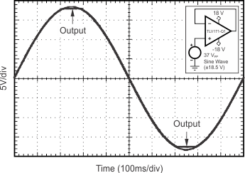
OPA171 OPA2171 OPA4171 No Phase ReversalFigure 6-1 No Phase Reversal
Table 6-1 Typical Performance Range
PARAMETERMINTYPMAXUNIT
Input common-mode voltage(V+) – 2(V+) + 0.1V
Offset voltage7mV
vs temperature12µV/°C
Common-mode rejection65dB
Open-loop gain60dB
GBW0.7MHz
Slew rate0.7V/µs
Noise at f = 1 kHz30nV/√ Hz