SBOS516H September 2010 – June 2024 OPA171 , OPA2171 , OPA4171
PRODUCTION DATA
4 Pin Configuration and Functions
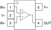 Figure 4-1 OPA171 DRL Package:
5-Pin SOT-553(Top View)
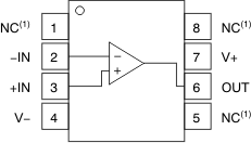
A. NC- no internal
connection
Figure 4-3 OPA171 D Package:
8-Pin SOIC(Top View)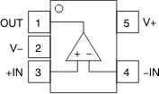 Figure 4-2 OPA171 DBV Package:
5-Pin SOT-23(Top View)
Figure 4-2 OPA171 DBV Package:
5-Pin SOT-23(Top View)Pin Functions: OPA171
| PIN | TYPE | DESCRIPTION | |||
|---|---|---|---|---|---|
| NAME | DRL | DBV | D | ||
| +IN | 1 | 3 | 3 | I | Noninverting input |
| –IN | 3 | 4 | 2 | I | Inverting input |
| OUT | 4 | 1 | 6 | O | Output |
| V+ | 5 | 5 | 7 | — | Positive (highest) supply |
| V– | 2 | 2 | 4 | — | Negative (lowest) supply |
| NC | — | — | 1, 5, 8 | — | No internal connection (can be left floating) |
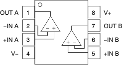 Figure 4-4 OPA2171 D, DCU, and DCK Packages:
8-Pin SO and VSSOP(Top View)
Figure 4-4 OPA2171 D, DCU, and DCK Packages:
8-Pin SO and VSSOP(Top View)Table 4-1 Pin Functions: OPA2171
| PIN | TYPE | DESCRIPTION | |
|---|---|---|---|
| NAME | NO. | ||
| +IN A | 3 | I | Noninverting input |
| +IN B | 5 | I | Noninverting input |
| –IN A | 2 | I | Inverting input |
| –IN B | 6 | O | Inverting input |
| OUT A | 1 | O | Output |
| OUT B | 7 | — | Output |
| V+ | 8 | — | Positive (highest) supply |
| V– | 4 | — | Negative (lowest) supply |
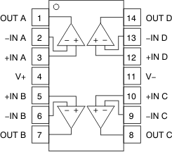 Figure 4-5 OPA4171 D and PW Packages:
14-Pin SO and TSSOP(Top View)
Figure 4-5 OPA4171 D and PW Packages:
14-Pin SO and TSSOP(Top View)Table 4-2 Pin Functions: OPA4171
| PIN | TYPE | DESCRIPTION | |
|---|---|---|---|
| NAME | NO. | ||
| +IN A | 3 | I | Noninverting input |
| +IN B | 5 | I | Noninverting input |
| +IN C | 10 | I | Noninverting input |
| +IN D | 12 | I | Noninverting input |
| –IN A | 2 | I | Inverting input |
| –IN B | 6 | I | Inverting input |
| –IN C | 9 | I | Inverting input |
| –IN D | 13 | I | Inverting input |
| OUT A | 1 | O | Output |
| OUT B | 7 | O | Output |
| OUT C | 8 | O | Output |
| OUT D | 14 | O | Output |
| V+ | 4 | — | Positive (highest) supply |
| V– | 11 | — | Negative (lowest) supply |