SBOS516H September   2010  – June 2024 OPA171 , OPA2171 , OPA4171

PRODUCTION DATA  

  1.   1
  2. Features
  3. Applications
  4. Description
  5. Pin Configuration and Functions
  6. Specifications
    1. 5.1 Absolute Maximum Ratings
    2. 5.2 ESD Ratings
    3. 5.3 Recommended Operating Conditions
    4. 5.4 Thermal Information: OPA171
    5. 5.5 Thermal Information: OPA2171
    6. 5.6 Thermal Information: OPA4171
    7. 5.7 Electrical Characteristics
    8. 5.8 Typical Characteristics: Table of Graphs
    9. 5.9 Typical Characteristics
  7. Detailed Description
    1. 6.1 Overview
    2. 6.2 Functional Block Diagram
    3. 6.3 Feature Description
      1. 6.3.1 Operating Characteristics
      2. 6.3.2 Common-Mode Voltage Range
      3. 6.3.3 Phase-Reversal Protection
      4. 6.3.4 Capacitive Load and Stability
    4. 6.4 Device Functional Modes
      1. 6.4.1 Common-Mode Voltage Range
  8. Application and Implementation
    1. 7.1 Application Information
      1. 7.1.1 Electrical Overstress
    2. 7.2 Typical Application
      1. 7.2.1 Design Requirements
      2. 7.2.2 Detailed Design Procedure
        1. 7.2.2.1 Capacitive Load and Stability
      3. 7.2.3 Application Curve
    3. 7.3 Power Supply Recommendations
    4. 7.4 Layout
      1. 7.4.1 Layout Guidelines
      2. 7.4.2 Layout Example
  9. Device and Documentation Support
    1. 8.1 Support Resources
    2. 8.2 Support Resources
    3. 8.3 Trademarks
    4. 8.4 Electrostatic Discharge Caution
    5. 8.5 Glossary
  10. Revision History
  11. 10Mechanical, Packaging, and Orderable Information

Description

The OPA171, OPA2171, and OPA4171 (OPAx171) are a family of 36V, single-supply, low-noise operational amplifiers with the ability to operate on supplies ranging from 2.7V (±1.35V) to 36V (±18V). These devices are available in micro-packages and offer low offset, drift, and bandwidth with low quiescent current. The single, dual, and quad versions all have identical specifications for maximum design flexibility.

Unlike most operational amplifiers, which are specified at only one supply voltage, the OPAx171 family is specified from 2.7V to 36V. Input signals beyond the supply rails do not cause phase reversal. The OPAx171 family is stable with capacitive loads up to 300pF. The input can operate 100mV below the negative rail and within 2V of the top rail during normal operation. These devices can operate with full rail-to-rail input 100mV beyond the top rail, but with reduced performance within 2V of the top rail.

The OPAx171 series of operational amplifiers are specified from –40°C to +125°C.

Package Information
PART NUMBER CHANNEL COUNT PACKAGE(1) PACKAGE SIZE(2)
OPA171 Single D (SOIC, 8) 4.9mm × 6mm
DBV (SOT-23, 5) 2.9mm × 2.8mm
DRL (SOT-5X3, 5) 1.6mm × 1.6mm
OPA2171 Dual D (SOIC, 8) 4.9mm × 6mm
DCU (VSSOP, 8) 2mm × 3.1mm
DGK (VSSOP, 8) 3mm × 4.9mm
OPA4171 Quad PW (TSSOP, 14) 5mm × 6.4mm
D (SOIC, 14) 8.65mm × 6mm
For all available packages, see the orderable addendum at the end of the data sheet.
The package size (length × width) is a nominal value and includes pins, where applicable.
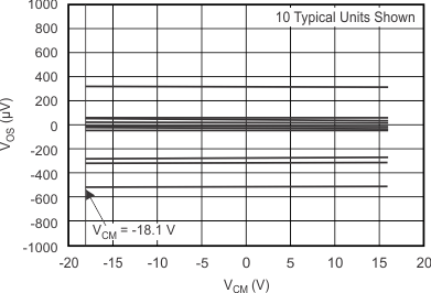
OPA171 OPA2171 OPA4171 Offset Voltage vs Common-Mode VoltageOffset Voltage vs Common-Mode Voltage
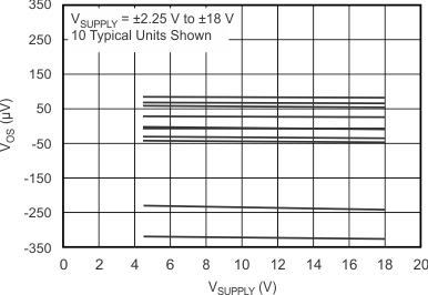
OPA171 OPA2171 OPA4171 Offset Voltage vs Power SupplyOffset Voltage vs Power Supply