SBOS622C July   2018  – January 2023 OPA855

PRODUCTION DATA  

  1. Features
  2. Applications
  3. Description
  4. Revision History
  5. Device Comparison Table
  6. Pin Configuration and Functions
  7. Specifications
    1. 7.1 Absolute Maximum Ratings
    2. 7.2 ESD Ratings
    3. 7.3 Thermal Information
    4. 7.4 Recommended Operating Conditions
    5. 7.5 Electrical Characteristics
    6. 7.6 Typical Characteristics
  8. Parameter Measurement Information
  9. Detailed Description
    1. 9.1 Overview
    2. 9.2 Functional Block Diagram
    3. 9.3 Feature Description
      1. 9.3.1 Input and ESD Protection
      2. 9.3.2 Feedback Pin
      3. 9.3.3 Wide Gain-Bandwidth Product
      4. 9.3.4 Slew Rate and Output Stage
    4. 9.4 Device Functional Modes
      1. 9.4.1 Split-Supply and Single-Supply Operation
      2. 9.4.2 Power-Down Mode
  10. 10Application, Implementation, and Layout
    1. 10.1 Application Information
    2. 10.2 Typical Application
      1. 10.2.1 Design Requirements
      2. 10.2.2 Detailed Design Procedure
      3. 10.2.3 Application Curves
    3. 10.3 Typical Application
      1. 10.3.1 Design Requirements
      2. 10.3.2 Detailed Design Procedure
      3. 10.3.3 Application Curves
    4. 10.4 Power Supply Recommendations
    5. 10.5 Layout
      1. 10.5.1 Layout Guidelines
      2. 10.5.2 Layout Example
  11. 11Device and Documentation Support
    1. 11.1 Device Support
      1. 11.1.1 Development Support
    2. 11.2 Documentation Support
      1. 11.2.1 Related Documentation
    3. 11.3 Receiving Notification of Documentation Updates
    4. 11.4 Support Resources
    5. 11.5 Trademarks
    6. 11.6 Electrostatic Discharge Caution
    7. 11.7 Glossary
  12. 12Mechanical, Packaging, and Orderable Information

Parameter Measurement Information

The various test setup configurations for the OPA855 are shown in Figure 8-1, Figure 8-2, and Figure 8-3. When configuring the OPA855 in a gain of +39.2 V/V, feedback resistor RF was set to 953 Ω.

Figure 7-1 shows 5-dB of peaking with the amplifier in an inverting configuration of –7 V/V with the amplifier configured as shown in Figure 8-2. The 50-Ω matched termination of this circuit configuration results in the amplifier being configured in a noise gain of 5.3 V/V, which is lower than the recommended +7 V/V.
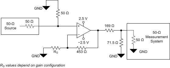
GUID-C4200420-68AD-4210-9603-4D349529E704-low.gifFigure 8-1 Noninverting Configuration
GUID-2577CB9C-B389-4CE8-A856-CB77CBBD27BB-low.gifFigure 8-2 Inverting Configuration (Gain = –7 V/V)
GUID-0F648E9C-ADC7-42FE-B934-8CCF5B5DB7BE-low.gifFigure 8-3 Capacitive Load Driver Configuration