SBOS743B July 2015 – September 2024 INA226-Q1
PRODUCTION DATA
- 1
- 1 Features
- 2 Applications
- 3 Description
- 4 Pin Configuration and Functions
- 5 Specifications
-
6 Detailed Description
- 6.1 Overview
- 6.2 Functional Block Diagram
- 6.3 Feature Description
- 6.4 Device Functional Modes
- 6.5 Programming
-
7 Registers
- 7.1
Register Maps
- 7.1.1 Configuration Register (00h) (Read/Write)
- 7.1.2 Shunt Voltage Register (01h) (Read-Only)
- 7.1.3 Bus Voltage Register (02h) (Read-Only) #GUID-792F23A7-1E45-4FB9-9334-0BF769622DE4/SBOS5477597
- 7.1.4 Power Register (03h) (Read-Only)
- 7.1.5 Current Register (04h) (Read-Only)
- 7.1.6 Calibration Register (05h) (Read/Write)
- 7.1.7 Mask/Enable Register (06h) (Read/Write)
- 7.1.8 Alert Limit Register (07h) (Read/Write)
- 7.1.9 Manufacturer ID Register (FEh) (Read-Only)
- 7.1.10 Die ID Register (FFh) (Read-Only)
- 7.1
Register Maps
- 8 Application and Implementation
- 9 Device and Documentation Support
- 10Revision History
- 11Mechanical, Packaging, and Orderable Information
6.4.1 Averaging and Conversion Time Considerations
The INA226-Q1 device offers programmable conversion times (tCT) for both the shunt voltage and bus voltage measurements. The conversion times for these measurements can be selected from as fast as 140 μs to as long as 8.244 ms. The conversion time settings, along with the programmable averaging mode, allow the device to be configured to optimize the available timing requirements in a given application. For example, if a system requires that data be read every 5ms, the device can be configured with the conversion times set to 588 μs for both shunt and bus voltage measurements and the averaging mode set to 4. This configuration results in the data updating approximately every 4.7ms. The device can also be configured with a different conversion time setting for the shunt and bus voltage measurements. This type of approach is common in applications where the bus voltage tends to be relatively stable. This situation can allow for the time focused on the bus voltage measurement to be reduced relative to the shunt voltage measurement. The shunt voltage conversion time can be set to 4.156 ms with the bus voltage conversion time set to 588 μs, with the averaging mode set to 1. This configuration also results in data updating approximately every 4.7 ms.
There are trade-offs associated with the settings for conversion time and the averaging mode used. The averaging feature can significantly improve the measurement accuracy by effectively filtering the signal. This approach allows the device to reduce any noise in the measurement that can be caused by noise coupling into the signal. A greater number of averages enables the device to be more effective in reducing the noise component of the measurement.
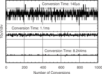
The conversion times selected can also have an impact on the measurement accuracy. Figure 6-2 shows multiple conversion times to illustrate the impact of noise on the measurement. to achieve the highest accuracy measurement possible, use a combination of the longest allowable conversion times and highest number of averages, based on the timing requirements of the system.
 Figure 6-2 Noise vs Conversion Time